General-Purpose Bus Controller
Élan™SC520 Microcontroller User’s Manual 13-9
:
13.5.2 I/O-Mapped and Memory-Mapped Device Support
The GP bus controller supports any combination of 8-bit and 16-bit I/O and memory-mapped
external devices.
■ If the external device is an I/O-mapped device, GPIORD and GPIOWR are used to
strobe the read and write accesses.
■ If the external device is a memory-mapped device, GPMEMRD and GPMEMWR are
used to strobe the read and write accesses.
To program I/O or memory-mapped address regions, see Chapter 4, “System Address
Mapping”, and the examples in “External GP Bus Devices” on page 3-13.
13.5.3 Chip Select Qualification
All GP bus chip selects can be qualified with the command strobes, GPIORD, GPIOWR,
GPMEMRD
, or GPMEMWR, by programming the GP Chip Select Qualification
(GPCSQUAL) register (MMCR offset C02h) and the Programmable Address Region (PAR)
registers for memory or I/O device selection.
When chip select qualification is enabled, the internal chip selects are logically ANDed with
one (or both) of these command strobes. If a single command is chosen for qualification,
the corresponding chip select is not asserted for accesses of the other type. For example,
if GPMEMWR
is used to exclusively qualify a chip select, that chip select is not asserted
for memory read accesses.
In a typical system environment, the command strobes are usually shorter than the chip
selects, and, in such cases, the external chip selects have timing that is identical to the
command strobes. Note that if the chip selects are internally qualified by commands, the
timing relationships between the command and chip select assertion/deassertion cannot
be guaranteed externally. For example, the chip select deassertion may lead the command
deassertion.
The qualification feature is useful for interfacing with buffer chips and transceivers without
requiring external gates or logic.
13.5.4 Data Sizing and Unaligned Accesses
The GP bus controller always operates in either 8-bit or 16-bit sizes. If the Am5
x
86 CPU
requests a 32-bit access from an 8-bit device or 16-bit device, the GP bus controller
responds to the Am5
x
86 CPU with bs8, indicating 8-bit data width, or bs16, indicating 16-
bit data width, depending on the programming of the GP Chip Select Data Width (GPCSDW)
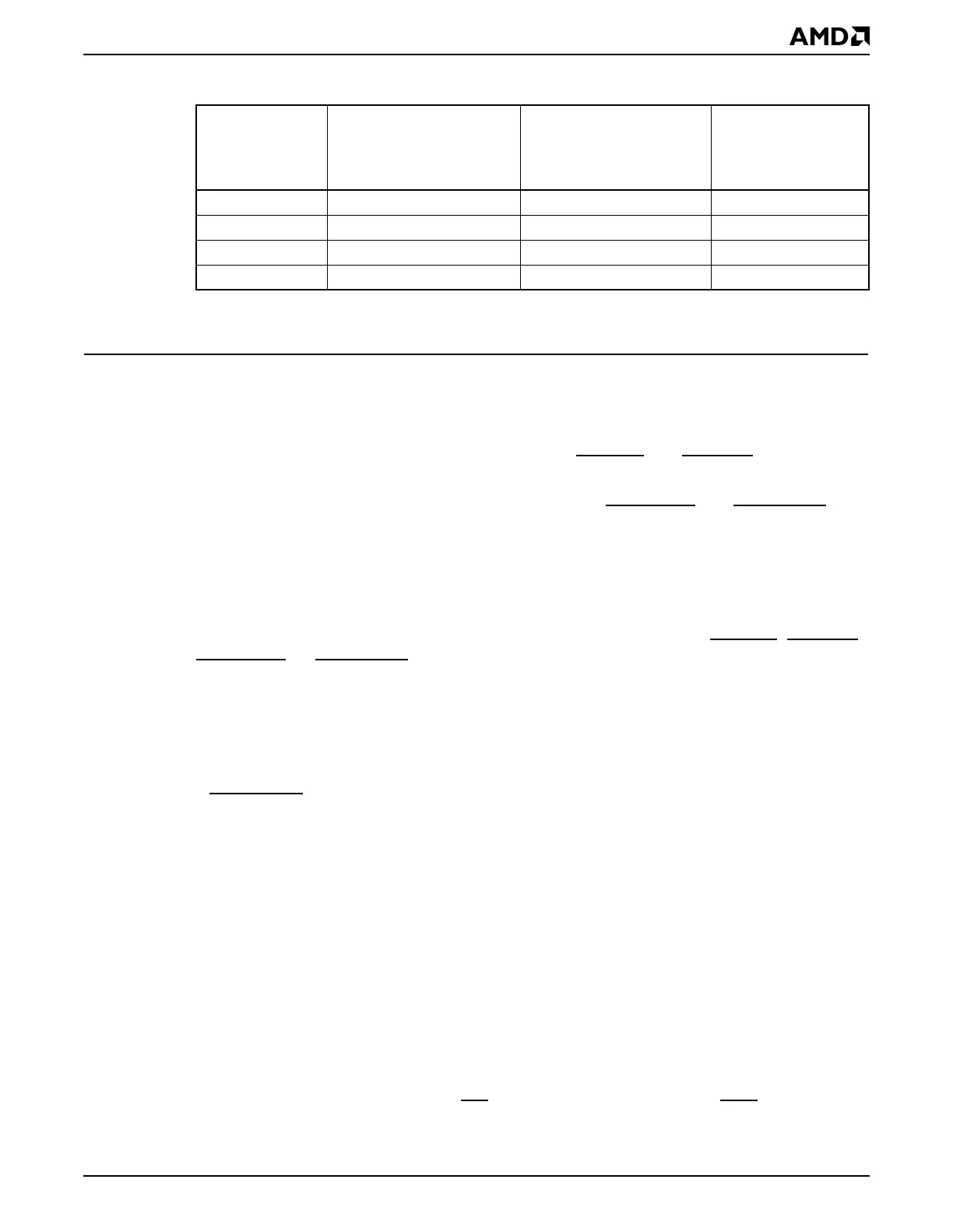
Table 13-3 GP Bus Echo Mode Minimum Timing
Signal Type
GPCSOFF, GPRDOFF,
GPALEOFF (Offset)
Register Value
1
Notes
1. The actual time value is the register value plus 1. Times are in units of one internal clock period.
GPCSPW, GPRDW,
GPALEW
(Pulse Width)
Register Value
1
GPCSRT
(Recovery Time)
Register Value
1
GP chip select 1 3 1
GP read 1 3 —
GP write 1 3 —
GPALE 0 0 —