Clock Generation and Control
5-6 Élan™SC520 Microcontroller User’s Manual
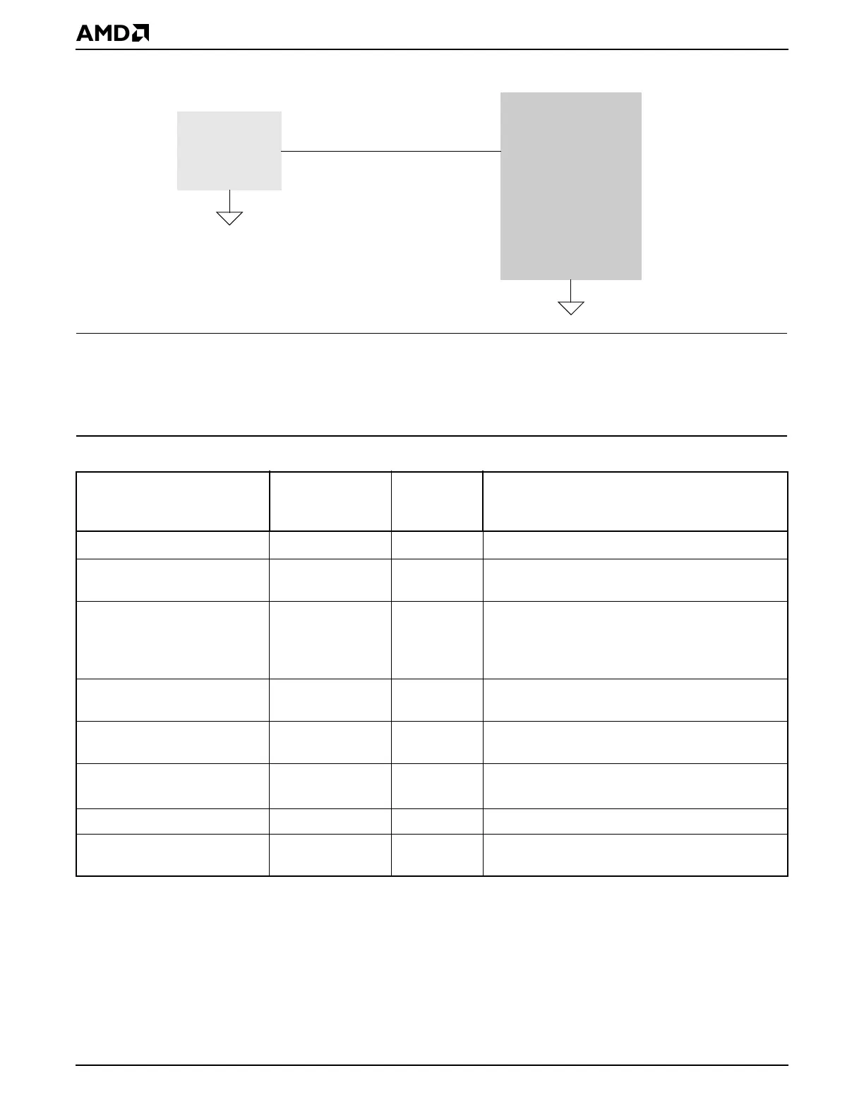
Figure 5-4 Bypassing the 33-MHz Oscillator
5.4 REGISTERS
A summary listing of the memory-mapped configuration registers used to control the clocks
on the ÉlanSC520 microcontroller is shown in Table 5-4.
Table 5-4 Clock Control Registers—Memory-Mapped
Register Mnemonic
MMCR
Offset
Address Function
Am5
x
86 CPU Control CPUCTL 02h CPU clock speed control
Software Timer Configuration SWTMRCFG 64h Crystal frequency (33.000 MHz or 33.333 MHz)
for software timer
Clock Select CLKSEL C26h CLKTIMER[CLKTEST] pin enable, clock output
select options (
18.432 MHz or 1.8432 MHz
UART, PLL1, PLL2, PIT, and RTC), CLKTIMER
or CLKTEST select
GP Timer 0 Mode/Control GPTMR0CTL C72h GP Timer 0: internal clock source prescaler,
external clock source
GP Timer 1 Mode/Control GPTMR1CTL C7Ah GP Timer 1: internal clock source prescaler,
external clock source
UART 1 General Control
UART 2 General Control
UART1CTL
UART2CTL
CC0h, CC4h UARTx clock source: 1.8432 MHz or 18.432
MHz
SSI Control SSICTL CD0h SSI clock speed
GP-DMA Control GPDMACTL D80h GP-DMA clock frequency: 4 MHz, 8 MHz, or 16
MHz
External
33-MHz
Oscillator
No Connect
33MXTAL2
33MXTAL1
Élan™SC520
Microcontroller
2.5-V max