SDRAM Controller
10-4 Élan™SC520 Microcontroller User’s Manual
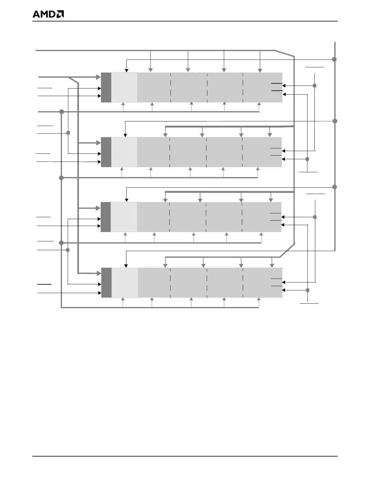
Figure 10-3 SDRAM Bank Configuration
Notes:
* ECC is optional. Since the entire doubleword is always written to the SDRAM during a read-modify-write operation
(see “Error Correction Code (ECC)” on page 10-16), any one of the four SDQM signals can be connected to the
DQM of the device that stores the 7-bit check word.
D[31:24] D[23:16] D[15:8] D[7:0]
Bank 3
Bank 1
Bank 2
Bank 0
SWEB
MA12–MA0,
MD31–MD0
MECC6–MECC0
SWEA
SDQM3–
DQM[0]
D[38:32]
SCS2
SCS1
SCS0
SCASB
SRASB
SCASA
SRASA
SCS3
CAS
RAS
DQM[1]
DQM[2]
DQM[3]
DQM[3]*
D[31:24] D[23:16] D[15:8] D[7:0]
DQM[0]
D[38:32]
CAS
RAS
DQM[1]
DQM[2]
DQM[3]
DQM[3]*
D[31:24] D[23:16] D[15:8] D[7:0]
DQM[0]
D[38:32]
CAS
RAS
DQM[1]
DQM[2]
DQM[3]
DQM[3]*
D[31:24] D[23:16] D[15:8] D[7:0]
DQM[0]
D[38:32]
CAS
RAS
DQM[1]
DQM[2]
DQM[3]
DQM[3]*
BA1–BA0
SDQM0