ROM/Flash Controller
Élan™SC520 Microcontroller User’s Manual 12-5
12.4 REGISTERS
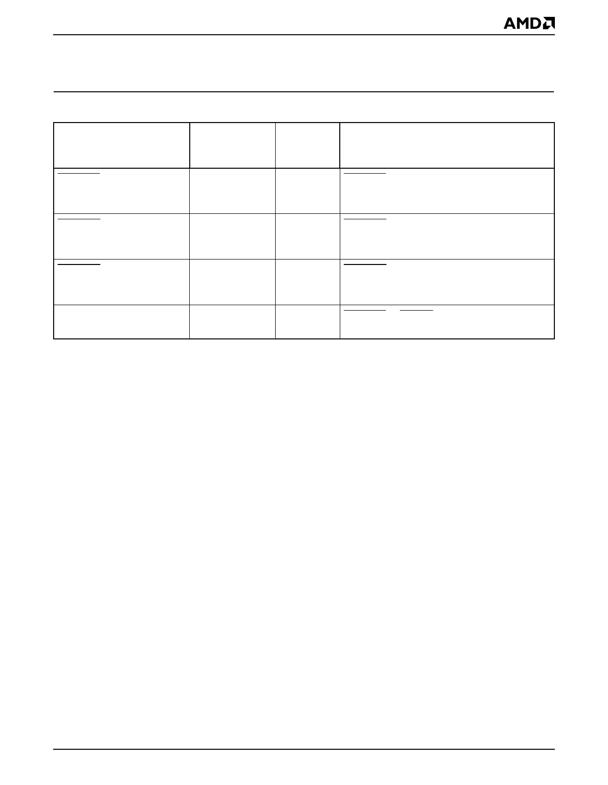
Table 12-3 shows the memory-mapped registers used to configure the ROM controller.
12.5 OPERATION
ROM/Flash devices in a system are typically used to store two different kinds of information:
system configuration data and program code. These applications impose different
constraints on how to use the ROM/Flash memory in the system.
While it may be sufficient to load system configuration information from ROM/Flash at a
low speed, this may be not acceptable for accessing ROM-resident code that has to be
executed. In this case, this code has to be copied either to SDRAM or executed directly
from ROM. (See Chapter 3, “System Initialization” for more information on shadowing.)
For copying code blocks, the ROM performance may not be critical, because it is only
accessed once per copy operation. For the more critical situation of executing code directly
from the ROM (e.g., an Execute-In-Place operating system), precautions have to be taken
to ensure an accelerated ROM access even for ROM devices incapable of bursting.
This chapter discusses different configurations and operating modes that are appropriate
for these varying situations.
12.5.1 ROM Support
Each of the three chip selects included on the ÉlanSC520 microcontroller supports up to
64 Mbytes. Some example configurations for each chip select are:
■ Four 1-Mbit x 8 devices on the 32-bit SDRAM data bus for a total of 4 Mbytes
■ Two banks of ROM, with each bank containing four 8-Mbit x 8 devices, providing a total
of 64 Mbytes
■ Two banks of ROM, with each bank containing two 8-Mbit x 16 devices, providing a total
of 64 Mbytes
■ Four banks of ROM, with each bank containing two 8-Mbit x 8 devices, providing a total
of 64 Mbytes
Table 12-3 ROM Controller Registers—Memory-Mapped
Register Mnemonic
MMCR
Offset
Address Function
BOOTCS
Control BOOTCSCTL 50h BOOTCS device select (SDRAM bus or GP
bus), device data width, device operation mode,
subsequent access delay, first access delay
ROMCS1
Control ROMCS1CTL 54h ROMCS1 device select (SDRAM bus or GP
bus), device data width, device operation mode,
subsequent access delay, first access delay
ROMCS2
Control ROMCS2CTL 56h ROMCS2 device select (SDRAM bus or GP
bus), device data width, device operation mode,
subsequent access delay, first access delay
Chip Select Pin Function
Select
CSPFS C24h ROMCSx
or GPCSx pin function select