System Test and Debugging
24-8 Élan™SC520 Microcontroller User’s Manual
24.4.2.2 SDRAM Write Cycle in Write Buffer Test Mode
Table 24-3 describes the WBMSTR2
±
WBMSTR0 decoding during an SDRAM write
operation.
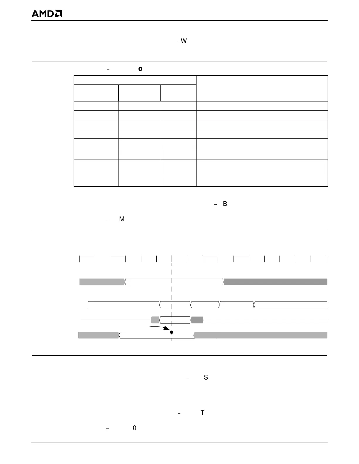
Figure 24-3 illustrates the timing of an example of a page hit SDRAM write cycle during
write buffer test mode. To capture the WBMSTR2
±
WBMSTR0 pins, the logic analyzer or
external in-circuit emulation system must decode the SDRAM command and latch the
WBMSTR2
±
WBMSTR0 pin on the rising edge of CLKMEMIN.
Figure 24-3 Write Buffer Test Mode Timing During an SDRAM Write Cycle (Page Hit)
24.4.2.3 SDRAM Read Cycle in Write Buffer Test Mode
During read operations, the WBMSTR2
±
WBMSTR0 pins can be used to determine which
master is performing the current SDRAM read cycle. Although more than one of these
sources may have written to a given rank in the write buffer, only one initiator can read a
rank at any given time.
Table 24-4 describes the WBMSTR2
±
WBMSTR0 pins during a SDRAM read operation in
write buffer test mode. Note that SDRAM read cycles can occur with more than one of the
WBMSTR2
±
WBMST0 signals active during the read portion of a read-modify-write cycle.
Table 24-3 WBMSTR2
±
WBMSTR0 Pin Definition During Write Buffer Write Cycles
WBMSTR2
±
WBMSTR0 Pins
Description
Am5
x
86 CPU
PCI
Bus Master
GP-DMA
Controller
0 0 0 Reserved
0 0 1 GP-DMA contributed write data
0 1 0 PCI master contributed write data
0 1 1 PCI master and GP-DMA contributed write data
100Am5
x
86 CPU contributed write data
101Am5
x
86 CPU and GP-DMA contributed write data
110Am5
x
86 CPU and PCI master contributed write
data
1 1 1 All masters contributed write data
CLKMEMIN
BA1–BA0
Command
MD31–MD0
Wr
Nop
Nop
WBMSTR2–
Sample WBMSTRx pins here
WBMSTR0
MA12–MA0