System Test and Debugging
Élan™SC520 Microcontroller User’s Manual 24-5
Figure 24-1 System Test Mode Timing During a SDRAM Write Cycle (Page Hit)
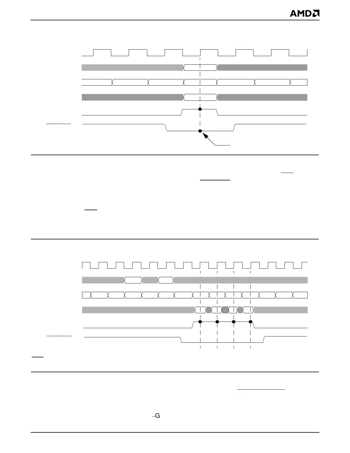
24.4.1.4 SDRAM Read Cycle in System Test Mode
Figure 24-2 illustrates the timing of a page miss SDRAM read cycle (with a CAS Latency
of 2) during system test mode. To capture the CF_DRAM
, BA1–BA0, MA12–MA0, and
MD31–MD0 signals, the logic analyzer or external in-circuit emulation system can use the
DATASTRB signal to identify the appropriate time to latch the information. This information
must be captured on the rising edge of CLKMEMIN when DATASTRB is sampled active.
The CAS
latency timing is configured in the SDRAM Timing Control (DRCTMCTL) register
(MMCR offset 12h). The BA1–BA0 and MA12–MA0 bus can be used to determine the
physical address generated by the requesting master.
Figure 24-2 System Test Mode Timing During an SDRAM Read Cycle (Page Miss)
24.4.1.5 Tracing Transactions on the ROM Interface
Tracing transactions on the ROM interface requires only the CF_ROM_GPCS signal if it is
desired to differentiate code fetches from memory read cycles. Only the Am5
x
86 CPU can
be the initiator of ROM accesses. The address bus is non-multiplexed, and thus can be
read directly from the GPA25
±
GPA0 pins during ROM/Flash cycles. The system
Nop Wr Nop
Col
a
CLKMEMIN
BA1–BA0
MD31–MD0
DATASTRB
CF_DRAM
Valid on this clock edge
Command
MA12–MA0
Nop RdAct Nop Nop
abcd
Row Col
CLKMEMIN
BA1–BA0
Command
MD31–MD0
DATASTRB
CF_DRAM
MA12–MA0
Notes:
CAS
latency is 2.