General-Purpose Bus Controller
13-6 Élan™SC520 Microcontroller User’s Manual
13.5 OPERATION
The GP bus provides a simple interface to the integrated on-chip peripherals, as well as
external peripherals. The GP bus operates at 33 MHz.
The GP bus controller provides one
fixed
timing set for the internal peripherals and one
programmable
timing set for the external peripherals.
Internal to the ÉlanSC520 microcontroller, the GP bus is used to provide a full complement
of integrated peripherals such as a DMA controller, programmable interrupt controller PIC),
programmable interval timer (PIT), UARTs, and real-time clock (RTC). The internal
peripherals are designed to operate at the full clock rate of the GP bus. They can also be
configured to operate in PC/AT-compatible configuration, but are generally not restricted
to this configuration.
The GP bus interface can be programmed by software to control the interface timing
between the GP bus and the external devices. The GP bus interface supports
programmable timing, dynamic data width sizing, and cycle stretching to accommodate a
wide variety of standard peripherals.
Eight chip selects are provided for external GP bus devices. They can be used for either
memory or I/O accesses. These chip selects are asserted for Am5
x
86 CPU accesses to
the corresponding regions set up in the Programmable Address Region (PAR) registers.
Four external DMA channels provide fly-by DMA transfers between peripheral devices on
the GP bus and system SDRAM.
GP bus accesses can be initiated only by the Am5
x
86 CPU or by the integrated GP bus
DMA controller. The devices on the GP bus are not cacheable from the Am5
x
86 CPU’s
viewpoint, to enable a simple user view of devices (memory and peripherals) that are located
on the GP bus.
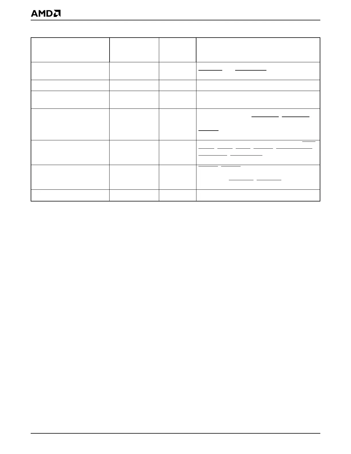
GP Write Offset GPWROFF C0Eh Offset from the beginning of the bus cycle for
GPIOWR
and GPMEMWR
GP ALE Pulse Width GPALEW C0Fh Width of the GPALE signal from the offset
GP ALE Offset GPALEOFF C10h Offset from the beginning of the bus cycle for
GPALE
PIO15–PIO0 Pin Function
Select
PIOPFS15_0 C20h PIO15–PIO0 or interface function select:
GPIRQ10–GPIRQ8, GPDACK3
–GPDACK0,
GPDRQ3–GPDRQ3, GPTC, GPAEN, GPRDY,
GPBHE
, GPALE
PIO31–PIO16 Pin Function
Select
PIOPFS31_16 C22h PIO31–PIO16 or interface function select: RIN2
,
DCD2
, DSR2, CTS2, GPCS0, GPMEMCS16,
GPIOCS16
, GPDBUFOE, GPIRQ7–GPIRQ0
Chip Select Pin Function
Select
CSPFS C24h GPCS7
–GPCS1 or alternate function select:
TMROUT1–TMROUT0, TMRIN1–TMRIN0,
PITGATE2, ROMCS2
, ROMCS1
Reset Configuration RESCFG D72h
Control bit for
GP bus reset (GPRESET)
Table 13-2 GP Bus Registers—Memory-Mapped (Continued)
Register Mnemonic
MMCR
Offset
Address Function
 Loading...