System Test and Debugging
Élan™SC520 Microcontroller User’s Manual 24-9
In this case, the WBMSTR2
±
WBMSTR0 pins represent which bus initiators contributed to
the rank of the write buffer that is being written to SDRAM.
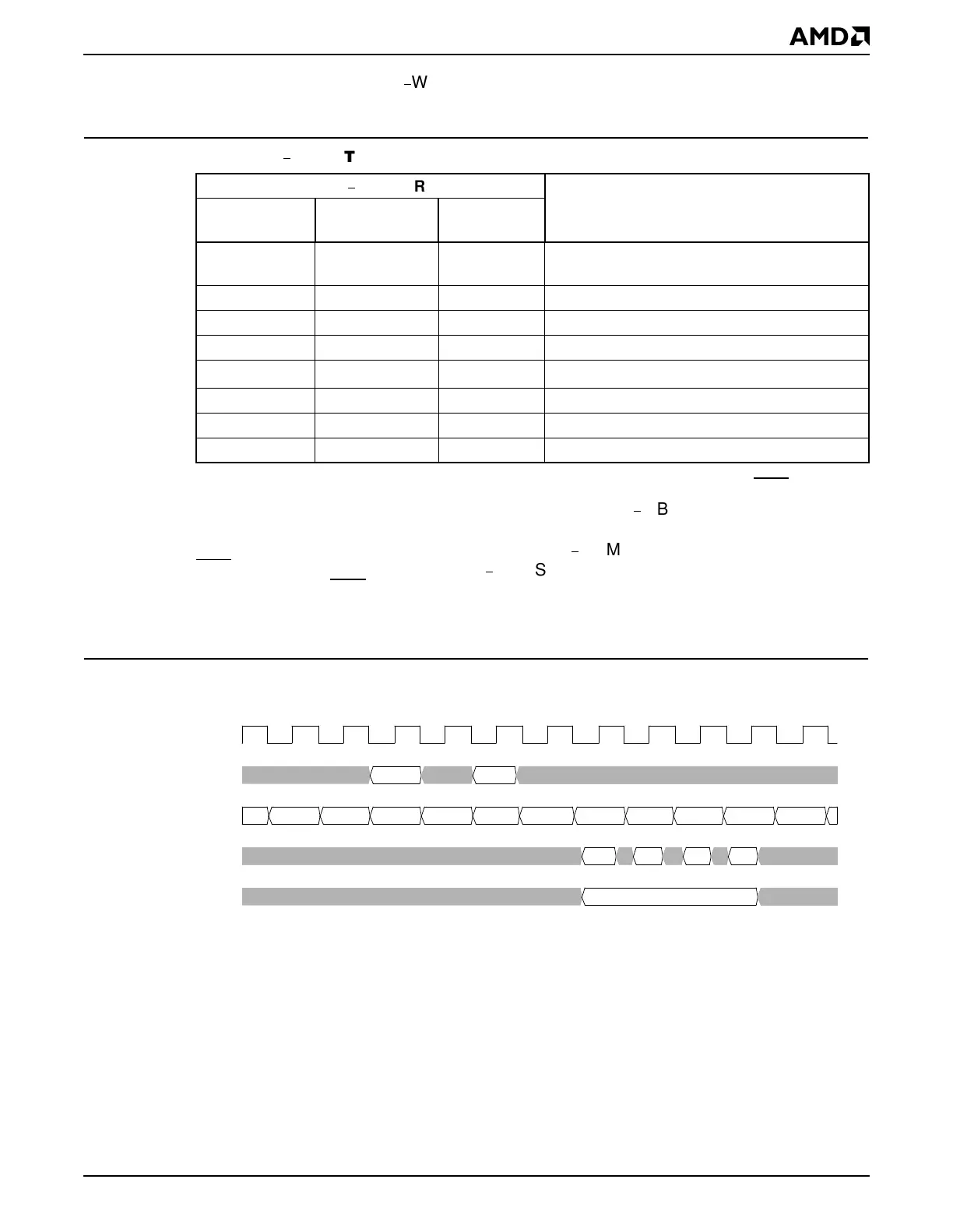
Figure 24-4 illustrates the timing of a page miss SDRAM read cycle (with a CAS latency of
2) during write buffer test mode. To capture the WBMSTR2
±
WBMSTR0 pins during a read
cycle, the logic analyzer or external in-circuit emulation system must decode the SDRAM
read command and delay latching the WBMSTR2
±
WBMSTR0 pins until the appropriate
CAS
latency timing is met. WBMSTR2
±
WBMSTR0 are captured on the rising edge of
CLKMEMIN. The CAS
latency timing is configured in the SDRAM Timing Control
(DRCTMCTL) register (MMCR offset 12h). The MA12–MA0 and BA1–BA0 signals can be
used to determine the physical address generated by the requesting master.
Figure 24-4 Write Buffer Test Mode Timing During a SDRAM Read Cycle (Page Miss)
Table 24-4 WBMSTR2
±
WBMSTR0 Pin Definition During SDRAM Read Cycles
WBMSTR2
±
WBMSTR0 Pins
Description
Am5
x
86 CPU
PCI
Bus Master
GP-DMA
Controller
0 0 0 Read prefetch cycle (No master requested
read cycle)
0 0 1 GP-DMA is current read master
0 1 0 PCI master is current read master
0 1 1 Reserved
10 0Am5
x
86 CPU is current read master
1 0 1 Reserved
1 1 0 Reserved
1 1 1 Reserved
Nop RdAct Nop Nop
abc d
Row Col
CPU
CLKMEMIN
BA1–BA0
MD31–MD0
WBMSTR2–
WBMSTR0
Command
MA12–MA0