General-Purpose Bus Controller
13-18 Élan™SC520 Microcontroller User’s Manual
13.5.9.4 32-Bit Data Access of an 8-Bit I/O Device
A 32-bit data access of an 8-bit I/O device requires four consecutive 8-bit data accesses
of the 8-bit I/O device, but the consecutive 8-bit data accesses are resolved by the Am5
x
86
CPU transparent to software. For memory-mapped I/O accesses, GPMEMRD
and
GPMEMWR
are used instead of GPIORD and GPIOWR. When the Am5
x
86 CPU requests
a 32-bit data access, the GP bus controller responds to the Am5
x
86 CPU with the bs8
signal, indicating that data width of the device is only 8 bits. The Am5
x
86 CPU then
generates four consecutive 8-bit bus cycles, and the 32-bit data access becomes four
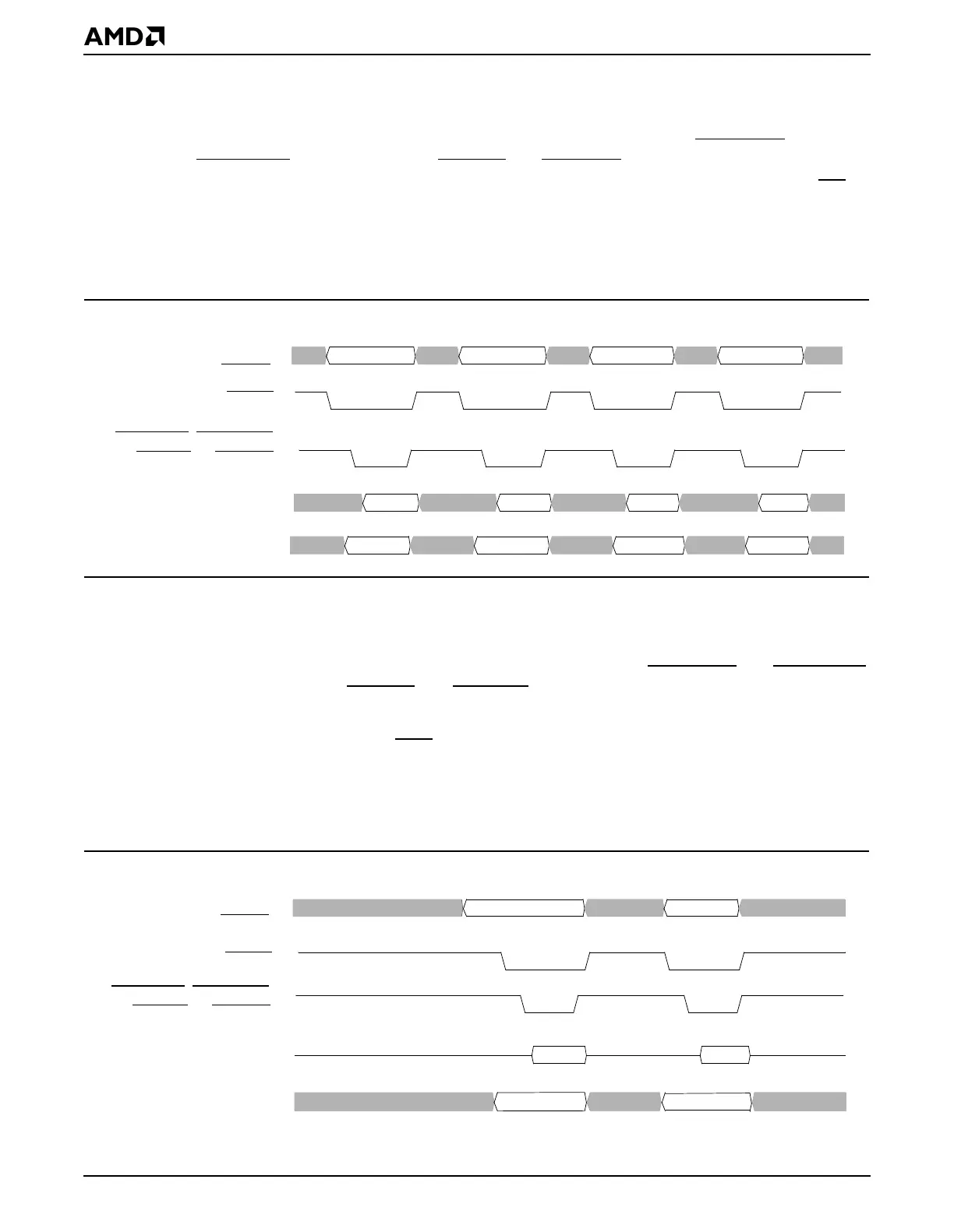
separate 8-bit data GP bus cycles. Figure 13-12 shows the timing diagram of a 32-bit access
of an 8-bit I/O device.
Figure 13-12 32-Bit Data Access of an 8-Bit I/O Device
13.5.9.5 32-Bit Data Access of a 16-Bit I/O Device
A 32-bit data access of a 16-bit I/O device requires two consecutive 16-bit accesses of the
device, but the consecutive 16-bit data accesses are resolved by the Am5
x
86 CPU
transparent to software. For memory-mapped I/O accesses, GPMEMRD
and GPMEMWR
are used instead of GPIORD
and GPIOWR.
When the Am5
x
86 CPU requests a 32-bit data access, the GP bus controller responds to
the Am5
x
86 CPU with the bs16 signal, indicating that the data width of the device is only
16 bits. The Am5
x
86 CPU then generates two consecutive 16-bit bus cycles, and the 32-
bit data access becomes two separate 16-bit cycles on the GP bus.
Figure 13-13 shows the timing diagram of a 32-bit access of a 16-bit I/O device.
Figure 13-13 32-Bit Data Access of a 16-Bit I/O Device
1st 2nd 3rd 4th
x..x0h x..x1h x..x2h x..x3h
GPA25–GPA0,
GPCSx
GPD7–GPD0
1st 2nd 3rd 4th
GPD7–GPD0
(for read)
for write
GPBHE
GPMEMRD, GPMEMWR,
GPIORD
, or GPIOWR
x..x0h
1st 2nd
x..x2h
GPA25–GPA0,
GPCSx
GPD15–GPD0
1st 2nd
GPD15–GPD0
GPBHE
(for write)
(for read)
GPMEMRD, GPMEMWR,
GPIORD, or GPIOWR