System Initialization
Élan™SC520 Microcontroller User’s Manual 3-15
3.7.5 PCI Bus Devices
Normally, devices on the PCI bus are mapped into memory space that is above the
configured amount of DRAM and just under 4 Gbytes (FFFEFFFFh). The ÉlanSC520
microcontroller’s address decode logic forwards all access to these memory locations to
the PCI bus.
Normally, memory cycles below the top address used by SDRAM are forwarded only to
the SDRAM controller, or to the GP bus if a PAR register is appropriately programmed.
However, for Windows and DOS compatibility, some PCI peripherals need to be mapped
into SDRAM space. These regions usually fall below the real-mode address limit (physical
address 0010FFEFh
). Devices that can require this include PCI-based VGA video cards
and PCI-based network adapters. To allow this, the first two PAR registers support the PCI
bus as a target. Note PCI as a target can only be specified in PAR 0 and PAR 1.
For such devices, a PAR register must be programmed that allows addresses lower than
the highest SDRAM address to be forwarded to the PCI bus. This is in addition to the normal
PCI bus device configuration. The VGA controller example in Section 3.7.5.1 illustrates this.
Typically, all I/O space accesses above the 1-Kbyte boundary are forwarded to the PCI
bus, and all I/O space accesses below the 1-Kbyte boundary are forwarded to the GP bus.
■ With some minor exceptions for the CBAR and PCI configuration registers, the I/O space
above the 1-Kbyte boundary can be redirected from the PCI to the GP bus using PAR
registers.
■ The IO_HOLE_DEST bit in the Address Decode Control (ADDDECCTL) register (MMCR
offset 80h) can be programmed to allow
all
I/O space addresses below the 1-Kbyte
boundary that are not assigned to internal peripherals to be forwarded to the PCI bus.
■ Note that PAR registers can still be mapped in the lower 1-Kbyte I/O space to override
the IO_HOLE_DEST bit. This way, I/O devices in the lower 1-Kbyte space can reside
internally to the ÉlanSC520 microcontroller, on the external GP-Bus, and on the PCI bus.
3.7.5.1 VGA Controller on the PCI Bus
A VGA video controller’s 128 Kbytes of memory is normally mapped from 000A0000–
000BFFFFh (physical addresses). So, to support a PCI-based video controller, PAR 0 or
PAR 1 would need to be programmed to 7200400Ah. This configures PAR 0 or PAR 1 with
the characteristics shown in Table 3-5. The attribute fields are ignored for the PCI bus target.
PCI regions are always writable, executable, and noncached.
A PCI VGA video adapter also requires PCI I/O from addresses 03B0–03BBh and 03C0–
03CFh. A PAR register is not required to map these I/O locations to PCI space, but instead
the IO_HOLES_DEST bit must be set in the Address Decode Control (ADDDECCTL)
register (MMCR offset 80h). This has the effect of mapping
all
external I/O accesses to PCI
space rather than to the GP bus. If there are no external GP bus I/O devices, then no further
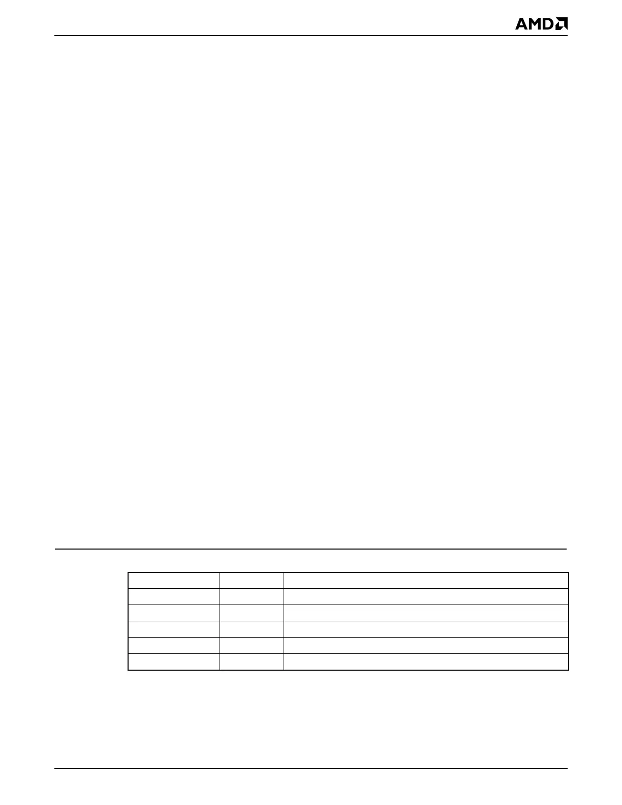
Table 3-5 Example PAR Programming: VGA Controller on the PCI Bus
Bit Field Value Meaning
Target Device 011b PCI bus
Attribute Field 000b Not applicable
Page Size 1b 64-Kbyte granularity
Region Size 1h Specifies two 64-Kbyte pages for a 128-Kbyte region size
Start Address Ah Physical address 000A0000h