System Initialization
Élan™SC520 Microcontroller User’s Manual 3-17
3.7.6 External ROM Devices
The PAR registers can also be used to define the addressing for ROM devices selected by
BOOTCS
, ROMCS1, and ROMCS2. ROM devices include true ROMs, EEPROM, Flash
devices, and other similar devices.
It is important to note that the top 64 Kbytes of the ROM device selected by BOOTCS
(the
boot device chip select) is
always
mapped to the physical addresses from FFFF0000–
FFFFFFFFh. This area is called the reset region. The reset region is cached, executable,
and not write-protected. This 64-Kbyte mapping is fixed and always active, even if the boot
ROM device is mapped to another address using a PAR register. ROM devices attached
to BOOTCS
, ROMCS1, or ROMCS2 can be mapped anywhere in physical address space
below 40000000h (1 Gbyte).
3.7.6.1 Boot ROM Device Mapping for BIOS Shadowing
A 512-Kbyte Flash device is a common boot ROM device for systems with a BIOS. One
way to shadow the BIOS is to map it below 00100000h so that it can be accessed by real-
mode code. This is easily done with a single PAR register. For shadowing purposes, a good
place to park the boot ROM device is at 00001000h, which is just above the interrupt vector
table. The value 89FC0001h configures the PAR register as shown in Table 3-8.
3.7.6.2 Two Banks of Flash for an Execute-In-Place (XIP) Operating System
A system has eight 8-Mbit byte-wide Flash devices. Four are on ROMCS1 and four on
ROMCS2
. These devices will be mapped into eight Mbytes of contiguous 32-bit address
space from 00400000–00BFFFFFh. This requires two PAR registers because two ROM
chip selects need to be used. This example uses PAR 4 and PAR 5. Note that in addition
to programming the PAR registers, the ROM chip selects need to be mapped to physical
pins.
The value A20FC040h for PAR 4 would setup ROMCS1
for the first bank of Flash. This
configures the PAR register with the characteristics shown in Table 3-9. The value
C20FC080h for PAR 5 would setup ROMCS2
for the first bank of Flash. This configures
the PAR register with the characteristics shown in Table 3-10.
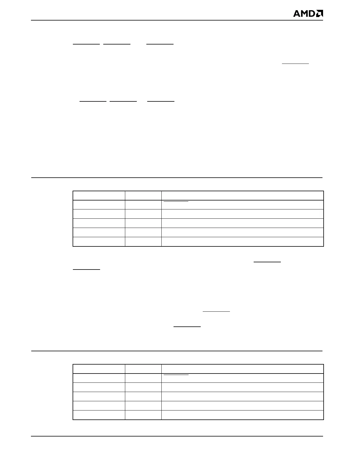
Table 3-8 Example PAR Programming: Boot ROM Device Mapping for BIOS Shadowing
Bit Field Value Meaning
Target Device 100b BOOTCS
Attribute Field 010b Write enable, noncacheable, code execution permitted
Page Size 0b 4-Kbyte granularity
Region Size 7Fh Specifies 128 4-Kbyte pages for a 512-Kbyte region size
Start Address 1h Physical address 00001000h
Table 3-9 Example PAR Programming: First Bank of Flash for XIP Operating System
Bit Field Value Meaning
Target Device 101b ROMCS1
Attribute Field 000b Write enable, cacheable, code execution allowed
Page Size 1b 64-Kbyte granularity
Region Size 3Fh Specifies sixty-four 64-Kbyte pages for a 4-Mbyte region size
Start Address 40h Physical address 00400000h