Write Buffer and Read Buffer
11-4 Élan™SC520 Microcontroller User’s Manual
are not shown in this table. When enabled, the multiplexed signals shown in Table 11-1
either disable or alter any other function that uses the same pin.
11.4 REGISTERS
The memory-mapped registers for SDRAM buffer control are shown in Table 11-2.
11.5 OPERATION
The write buffer and read buffer are two features implemented in the SDRAM controller to
increase SDRAM performance.
The write buffer provides a mechanism for
all
masters (Am5
x
86 CPU, PCI, or GP-DMA) to
post write data with zero wait states, thus decoupling the master from experiencing the
write latency penalty associated with the SDRAM. When the write buffer is enabled, all
write activity to SDRAM is initiated by the write buffer.
The read-ahead feature of the read buffer is designed to increase SDRAM read
performance by prefetching the cache line following the current access, thus possibly
supplying data to the requester with zero wait states. The read-ahead feature takes
advantage of the fetch-forward nature of the Am5
x
86 CPU prefetch engine (which relies
on spatial locality of program flow) and PCI read bursts. Read prefetching (when enabled)
occurs only for master read accesses that result in a burst of two or more doublewords. A
prefetch never occurs for a GP-DMA request since GP-DMA read requests are never burst.
However, during a GP-DMA read request, the remainder of the cache line is always fetched.
The write buffer provides a debug feature that, when enabled, provides contributing master
information on external pins (WBMSTR2–WBMSTR0) during a write buffer write cycle to
SDRAM. These pins reflect which master contributed to the write buffer level in the process
of being written back. The contributing masters reflected could be either: Am5
x
86 CPU,
PCI, or GP-DMA. Since the write buffer supports the write-merging and write-collapsing
functions, it is possible that multiple masters contributed to the same level that is in the
process of being written to SDRAM. See Chapter 24, “System Test and Debugging”, for
more information on write buffer debug support.
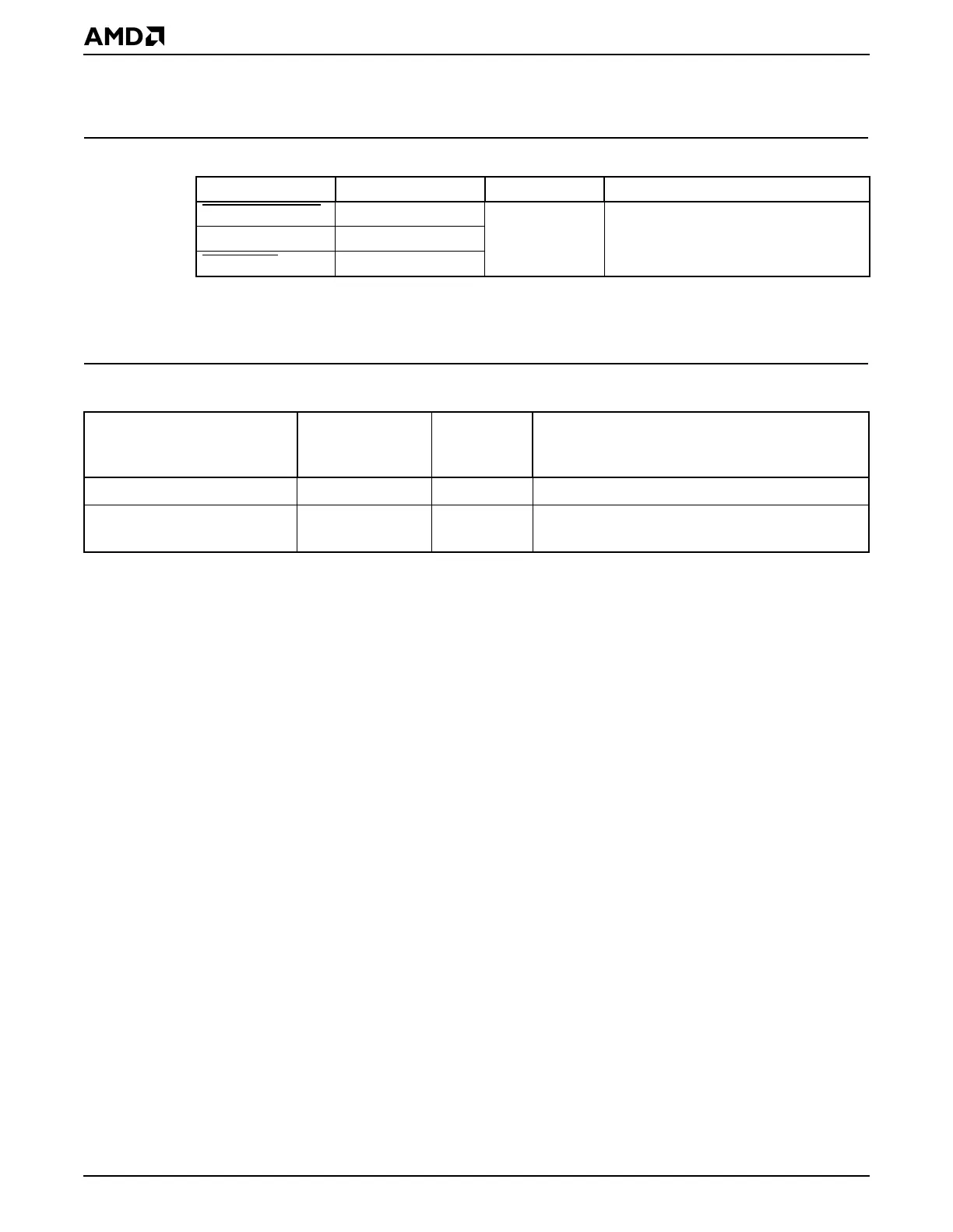
Table 11-1 SDRAM Signals Shared with Other Interfaces
Default Signal Alternate Function Control Bit Register
CF_ROM_GPCS
WBMSTR0 WB_TST_ENB SDRAM Control (DRCCTL) register
(MMCR offset 10h)
DATASTRB WBMSTR1
CF_DRAM
WBMSTR2
Table 11-2 SDRAM Buffer Control Registers—Memory-Mapped
Register Mnemonic
MMCR
Offset
Address Function
SDRAM Control DRCCTL 10h SDRAM write buffer test mode enable
SDRAM Buffer Control DBCTL 40h Write buffer enable, read-ahead enable, write
buffer watermark, write buffer flush