ROM/Flash Controller
12-8 Élan™SC520 Microcontroller User’s Manual
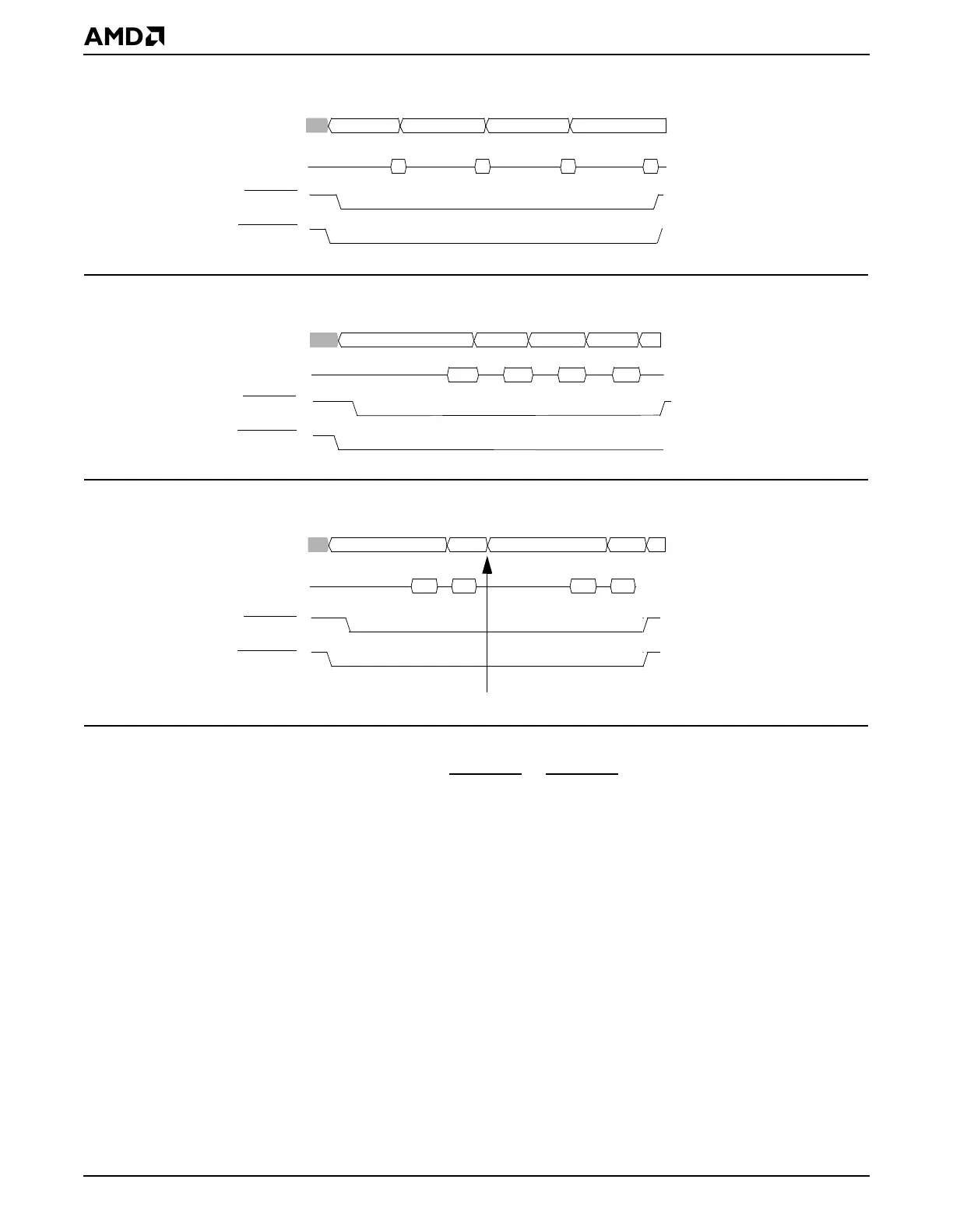
Figure 12-4 Non-Page-Mode ROM: Fetching Four Words from a 16-Bit ROM
Figure 12-5 Page-Mode ROM: Fetching Four Doublewords (Aligned) from a 32-Bit ROM
Figure 12-6 Page-Mode ROM: Fetching Four Doublewords (Unaligned) from an 8-Bit ROM
12.5.2.4 Access Timing
Access timing is controlled in the BOOTCS or ROMCSx Control registers.
– The delay for the first access, used for both non-page-mode and page-mode, and
subsequent accesses for non-page-mode is specified in the FIRST_DLY bit field.
– The delay for subsequent accesses, for page-mode only, is specified in the SUB_DLY
bit field.
Table 12-4 shows the access timing according to the programmed wait states. These values
can be obtained using the following formula:
AccessTime = (NumberWaitstates + 1) * Period –Setup)
where:
Period is the clock period (assume 30 ns for a 33.333-MHz crystal)
Setup is assumed to be 20 ns. (It takes the actual setup time and the delay for address
changes during subsequent ROM accesses into account.)
134
- - - 0h - - - 2h
- - - 4h
- - - 8h
GPA25–GPA0
GPD15–GPD0, or
ROMRD
BOOTCS
2
MD15–MD0
- - - 0h - - - 4h - - - 8h - - - ch
1234
GPA25–GPA0
MD31–MD0
ROMRD
BOOTCS
34 5
23 45
2
GPA25–GPA0
GPD7–GPD0, or
ROMRD
BOOTCS
Page crossing
MD7–MD0