General-purpose and alternate-function I/Os (GPIOs and AFIOs) RM0008
160/1096 Doc ID 13902 Rev 12
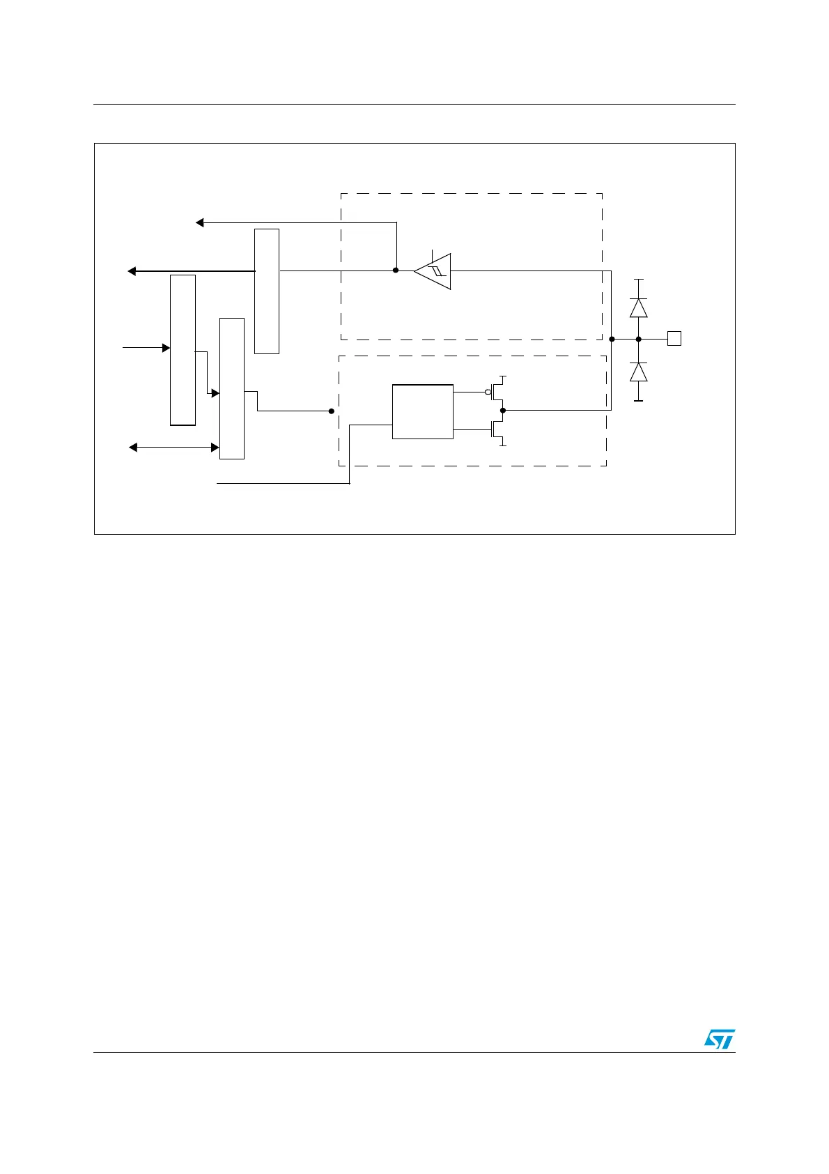
Figure 17. Alternate function configuration
1. V
DD_FT
is a potential specific to five-volt tolerant I/Os and different from V
DD
.
9.1.10 Analog configuration
When the I/O Port is programmed as Analog configuration:
● The Output Buffer is disabled.
● The Schmitt Trigger Input is de-activated providing zero consumption for every analog
value of the I/O pin. The output of the Schmitt Trigger is forced to a constant value (0).
● The weak pull-up and pull-down resistors are disabled.
● Read access to the Input Data Register gets the value “0”.
The Figure 18 on page 161 shows the high impedance-analog configuration of the I/O Port
bit.
Alternate Function Output
Alternate Function Input
push-pull or
open-drain
From on-chip
peripheral
To on-chip
peripheral
Output
control
I/O pin
V
DD
V
SS
TTL Schmitt
trigger
VSS
V
DD
or V
DD_FT
(1)
Protection
diode
Protection
diode
on
Input driver
Output driver
P-MOS
N-MOS
Input data register
Output data register
Read/write
Read
Bit set/reset registers
Write
ai14785
 Loading...


