RM0008 Basic timers (TIM6&TIM7)
Doc ID 13902 Rev 12 463/1096
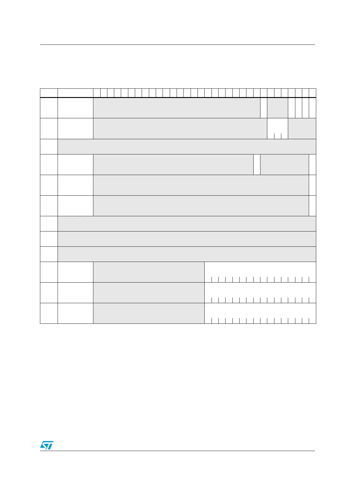
17.4.9 TIM6&TIM7 register map
TIMx registers are mapped as 16-bit addressable registers as described in the table below:
Refer to Table 3: Register boundary addresses for the register boundary addresses.
Table 94. TIM6&TIM7 register map and reset values
Offset Register
31
30
29
28
27
26
25
24
23
22
21
20
19
18
17
16
15
14
13
12
11
10
9
8
7
6
5
4
3
2
1
0
0x00
TIMx_CR1
Reserved
ARPE
Reserved
OPM
URS
UDIS
CEN
Reset value 00000
0x04
TIMx_CR2
Reserved
MMS[2:0]
Reserved
Reset value 000
0x08
Reserved
0x0C
TIMx_DIER
Reserved
UDE
Reserved
UIE
Reset value 00
0x10
TIMx_SR
Reserved
UIF
Reset value 0
0x14
TIMx_EGR
Reserved
UG
Reset value 0
0x18
Reserved
0x1C
Reserved
0x20
Reserved
0x24
TIMx_CNT
Reserved
CNT[15:0]
Reset value 0000000000000000
0x28
TIMx_PSC
Reserved
PSC[15:0]
Reset value 0000000000000000
0x2C
TIMx_ARR
Reserved
ARR[15:0]
Reset value 0000000000000000
 Loading...


