RM0008 Analog-to-digital converter (ADC)
Doc ID 13902 Rev 12 241/1096
11.12.14 ADC regular data register (ADC_DR)
Address offset: 0x4C
Reset value: 0x0000 0000
11.12.15 ADC register map
The following table summarizes the ADC registers.
Bits 31:16 Reserved, must be kept cleared.
Bits 15:0 JDATA[15:0]: Injected data
These bits are read only. They contain the conversion result from injected channel x. The
data is left or right-aligned as shown in Figure 27 and Figure 28.
31 30 29 28 27 26 25 24 23 22 21 20 19 18 17 16
ADC2DATA[15:0]
rrrrrrr r r r r r r r r r
15 14 13 12 11 10 9 8 7 6 5 4 3 2 1 0
DATA[15:0]
rrrrrrr r r r r r r r r r
Bits 31:16 ADC2DATA[15:0]: ADC2 data
In ADC1: In dual mode, these bits contain the regular data of ADC2. Refer to Section 11.9:
Dual ADC mode.
In ADC2 and ADC3: these bits are not used.
Bits 15:0 DATA[15:0]: Regular data
These bits are read only. They contain the conversion result from the regular channels. The
data is left or right-aligned as shown in Figure 27 and Figure 28.
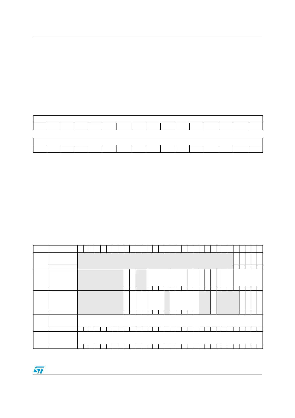
Table 72. ADC register map and reset values
Offset Register
31
30
29
28
27
26
25
24
23
22
21
20
19
18
17
16
15
14
13
12
11
10
9
8
7
6
5
4
3
2
1
0
0x00
ADC_SR
Reserved
STRT
JSTRT
JEOC
EOC
AWD
Reset value 00000
0x04
ADC_CR1
Reserved
AWDEN
JAWDEN
Reserved
DUALMOD
[3:0]
DISC
NUM [2:0]
JDISCEN
DISCEN
JAUTO
AWD SGL
SCAN
JEOC IE
AWDIE
EOCIE
AWDCH[4:0]
Reset value 00 00000000000000000000
0x08
ADC_CR2
Reserved
TSVREFE
SWSTART
JSWSTART
EXTTRIG
EXTSEL
[2:0]
Reserved
JEXTTRIG
JEXTSEL
[2:0]
ALIGN
Reserved
DMA
Reserved
RSTCAL
CAL
CONT
ADON
Reset value 0000000 00000 0 0000
0x0C
ADC_SMPR1 Sample time bits SMPx_x
Reset value 00000000000000000000000000000000
0x10
ADC_SMPR2 Sample time bits SMPx_x
Reset value 00000000000000000000000000000000
 Loading...


