Low-, medium-, high- and XL-density reset and clock control (RCC) RM0008
98/1096 Doc ID 13902 Rev 12
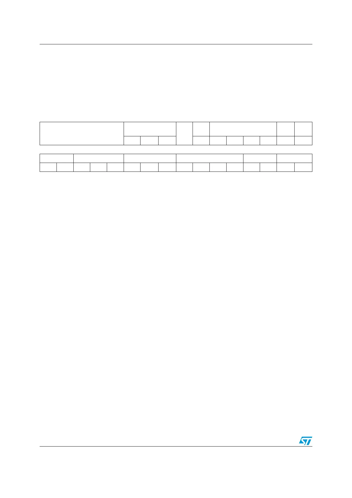
7.3.2 Clock configuration register (RCC_CFGR)
Address offset: 0x04
Reset value: 0x0000 0000
Access: 0 ≤ wait state ≤ 2, word, half-word and byte access
1 or 2 wait states inserted only if the access occurs during clock source switch.
31 30 29 28 27 26 25 24 23 22 21 20 19 18 17 16
Reserved
MCO[2:0]
Res.
USB
PRE
PLLMUL[3:0]
PLL
XTPRE
PLL
SRC
rw rw rw rw rw rw rw rw rw rw
15 14 13 12 11 10 9 8 7 6 5 4 3 2 1 0
ADCPRE[1:0] PPRE2[2:0] PPRE1[2:0] HPRE[3:0] SWS[1:0] SW[1:0]
rw rw rw rw rw rw rw rw rw rw rw rw r r rw rw
Bits 31:27 Reserved, always read as 0.
Bits 26:24 MCO: Microcontroller clock output
Set and cleared by software.
0xx: No clock
100: System clock (SYSCLK) selected
101: HSI clock selected
110: HSE clock selected
111: PLL clock divided by 2 selected
Note: This clock output may have some truncated cycles at startup or during MCO clock
source switching.
When the System Clock is selected to output to the MCO pin, make sure that this clock
does not exceed 50 MHz (the maximum IO speed).
Bit 22 USBPRE: USB prescaler
Set and cleared by software to generate 48 MHz USB clock. This bit must be valid before
enabling the USB clock in the RCC_APB1ENR register. This bit can’t be reset if the USB
clock is enabled.
0: PLL clock is divided by 1.5
1: PLL clock is not divided
 Loading...


