Secure digital input/output interface (SDIO) RM0008
584/1096 Doc ID 13902 Rev 12
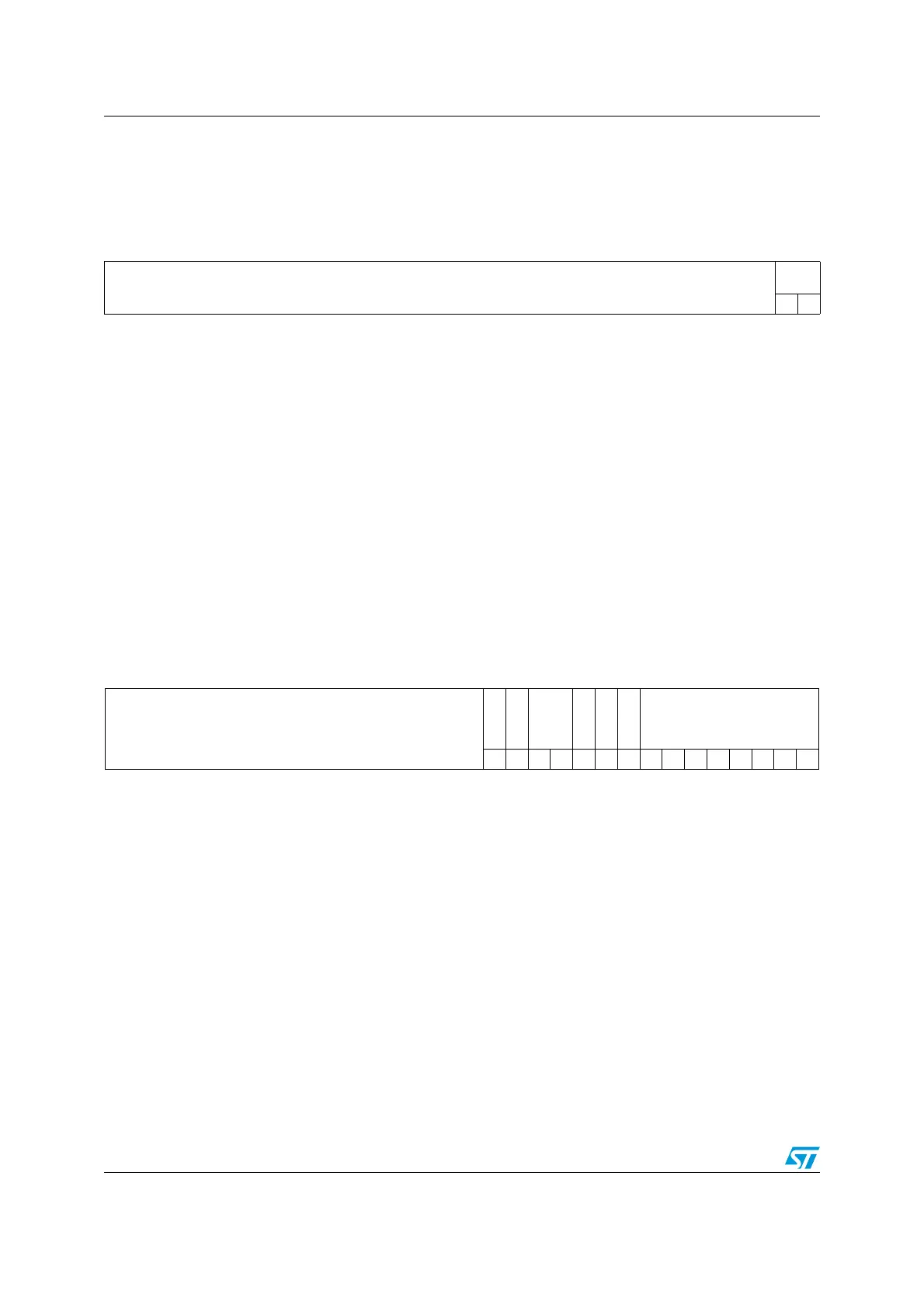
22.9.1 SDIO power control register (SDIO_POWER)
Address offset: 0x00
Reset value: 0x0000 0000
Note: At least seven HCLK clock periods are needed between two write accesses to this register.
22.9.2 SDI clock control register (SDIO_CLKCR)
Address offset: 0x04
Reset value: 0x0000 0000
The SDIO_CLKCR register controls the SDIO_CK output clock.
313029282726252423222120191817161514131211109876543210
Reserved
PWRC
TRL
rw rw
Bits 31:2 Reserved, always read as 0.
[1:0] PWRCTRL: Power supply control bits.
These bits are used to define the current functional state of the card clock:
00: Power-off: the clock to card is stopped.
01: Reserved
10: Reserved power-up
11: Power-on: the card is clocked.
313029282726252423222120191817161514131211109876543210
Reserved
HWFC_EN
NEGEDGE
WID
BUS
BYPASS
PWRSAV
CLKEN
CLKDIV
rw rw rw rw rw rw rw rw rw rw rw rw rw rw rw
Bits 31:15 Reserved, always read as 0.
Bit 14 HWFC_EN: HW Flow Control enable
0b: HW Flow Control is disabled
1b: HW Flow Control is enabled
When HW Flow Control is enabled, the meaning of the TXFIFOE and RXFIFOF interrupt
signals, please see SDIO Status register definition in Section 22.9.11.
Bit 13 NEGEDGE:SDIO_CK dephasing selection bit
0b: SDIO_CK generated on the rising edge of the master clock SDIOCLK
1b: SDIO_CK generated on the falling edge of the master clock SDIOCLK
Bits 12:11 WIDBUS: Wide bus mode enable bit
00: Default bus mode: SDIO_D0 used
01: 4-wide bus mode: SDIO_D[3:0] used
10: 8-wide bus mode: SDIO_D[7:0] used
 Loading...


