Serial peripheral interface (SPI) RM0008
690/1096 Doc ID 13902 Rev 12
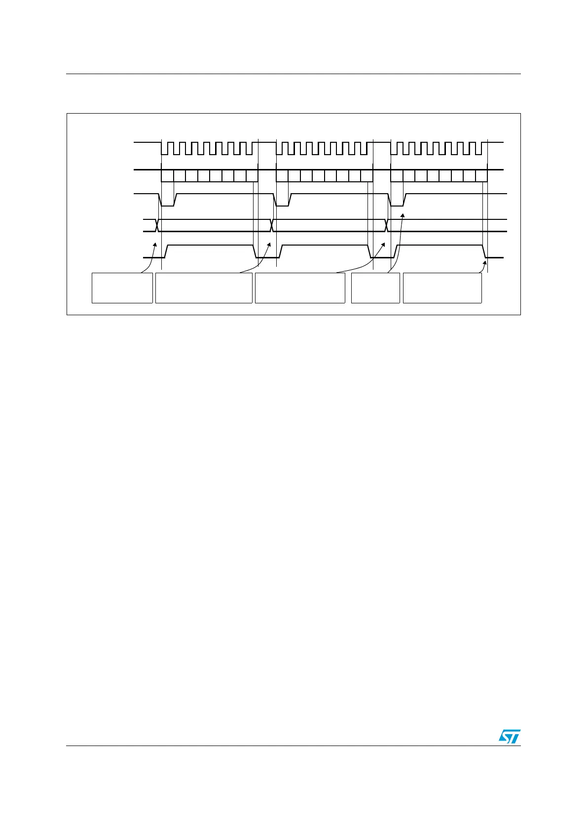
Figure 245. TXE/BSY behavior when transmitting (BIDIRMODE=0 and RXONLY=0) in the case of
discontinuous transfers
25.3.6 CRC calculation
A CRC calculator has been implemented for communication reliability. Separate CRC
calculators are implemented for transmitted data and received data. The CRC is calculated
using a programmable polynomial serially on each bit. It is calculated on the sampling clock
edge defined by the CPHA and CPOL bits in the SPI_CR1 register.
Note: This SPI offers two kinds of CRC calculation standard which depend directly on the data
frame format selected for the transmission and/or reception: 8-bit data (CR8) and 16-bit data
(CRC16).
CRC calculation is enabled by setting the CRCEN bit in the SPI_CR1 register. This action
resets the CRC registers (SPI_RXCRCR and SPI_TXCRCR). In full duplex or transmitter
only mode, when the transfers are managed by the software (CPU mode), it is necessary to
write the bit CRCNEXT immediately after the last data to be transferred is written to the
SPI_DR. At the end of this last data transfer, the SPI_TXCRCR value is transmitted.
In receive only mode and when the transfers are managed by software (CPU mode), it is
necessary to write the CRCNEXT bit after the second last data has been received. The
CRC is received just after the last data reception and the CRC check is then performed.
At the end of data and CRC transfers, the CRCERR flag in the SPI_SR register is set if
corruption occurs during the transfer.
If data are present in the TX buffer, the CRC value is transmitted only after the transmission
of the data byte. During CRC transmission, the CRC calculator is switched off and the
register value remains unchanged.
Note: Please refer to the product specifications for availability of this feature.
MOSI (out)
Tx buffer
DATA 1 = 0xF1
TXE flag
0xF1
BSY flag
0xF2
software writes 0xF1
into SPI_DR
software waits until TXE=1 but is
late to write 0xF2 into SPI_DR
software waits until TXE=1 but
is late to write 0xF3 into
SPI_DR
SCK
3Fx0 = 3 ATAD2Fx0 = 2 ATAD
Example with CPOL=1, CPHA=1
0xF3
software waits
until TXE=1
software waits until BSY=0
(write to SPI_DR)
b0 b1 b2 b3 b4 b5 b6 b7
b0 b1 b2 b3 b4 b5 b6 b7 b0 b1 b2 b3 b4 b5 b6 b7
ai17348
 Loading...


