Secure digital input/output interface (SDIO) RM0008
548/1096 Doc ID 13902 Rev 12
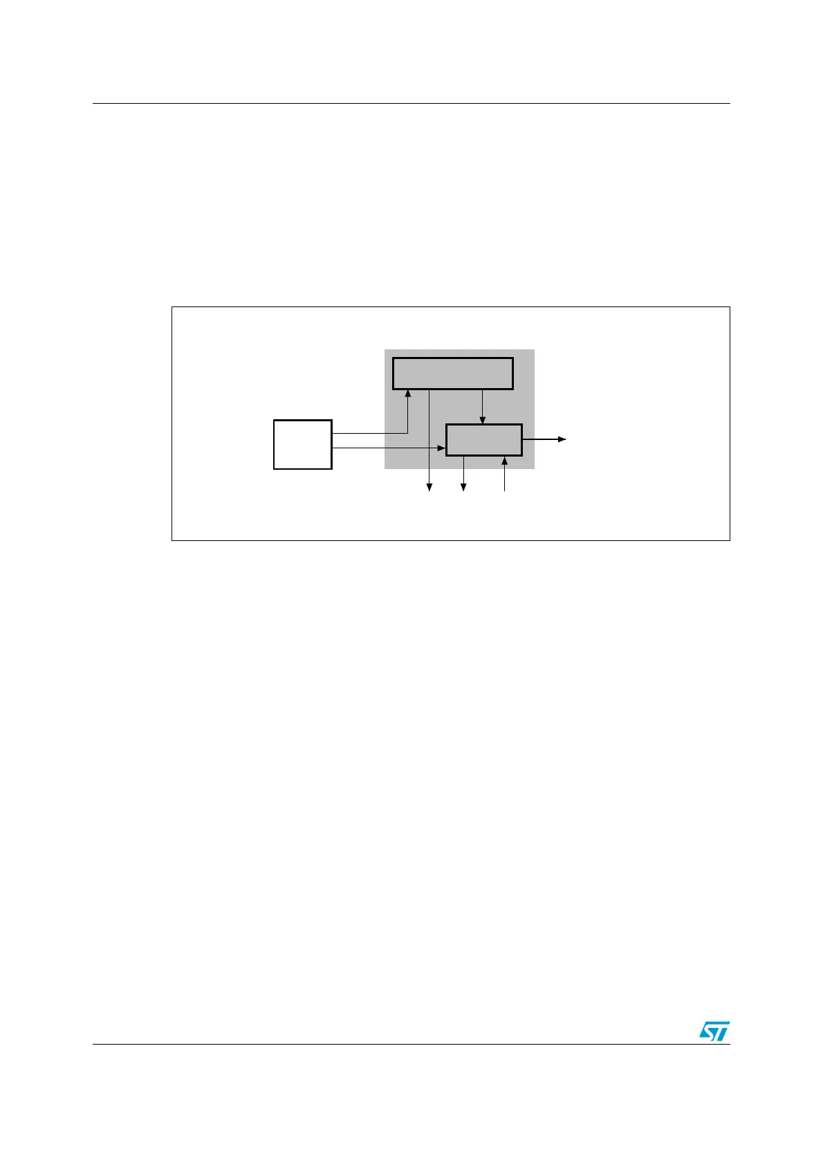
Control unit
The control unit contains the power management functions and the clock divider for the
memory card clock.
There are three power phases:
● power-off
● power-up
● power-on
Figure 213. Control unit
The control unit is illustrated in Figure 213. It consists of a power management subunit and
a clock management subunit.
The power management subunit disables the card bus output signals during the power-off
and power-up phases.
The clock management subunit generates and controls the SDIO_CK signal. The SDIO_CK
output can use either the clock divide or the clock bypass mode. The clock output is inactive:
● after reset
● during the power-off or power-up phases
● if the power saving mode is enabled and the card bus is in the Idle state (eight clock
periods after both the command and data path subunits enter the Idle phase)
Command path
The command path unit sends commands to and receives responses from the cards.
ai14804
Power management
Clock
management
Adapter
registers
SDIO_CK
Control unit
To command and data path
 Loading...


