Connectivity line devices: reset and clock control (RCC) RM0008
138/1096 Doc ID 13902 Rev 12
8.3.5 APB1 peripheral reset register (RCC_APB1RSTR)
Address offset: 0x10
Reset value: 0x0000 0000
Access: no wait state, word, half-word and byte access
Bit 4 IOPCRST: IO port C reset
Set and cleared by software.
0: No effect
1: Reset I/O port C
Bit 3 IOPBRST: IO port B reset
Set and cleared by software.
0: No effect
1: Reset I/O port B
Bit 2 IOPARST: I/O port A reset
Set and cleared by software.
0: No effect
1: Reset I/O port A
Bit 1 Reserved, always read as 0.
Bit 0 AFIORST: Alternate function I/O reset
Set and cleared by software.
0: No effect
1: Reset Alternate Function
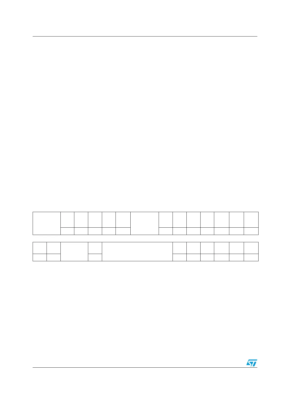
31 30 29 28 27 26 25 24 23 22 21 20 19 18 17 16
Reserved
DAC
RST
PWR
RST
BKP
RST
CAN2
RST
CAN1
RST
Reserved
I2C2
RST
I2C1
RST
UART
5
RST
UART
4
RST
USART
3
RST
USART
2
RST
Res.
rw rw rw rw rw rw rw rw rw rw rw
15 14 13 12 11 10 9 8 7 6 5 4 3 2 1 0
SPI3
RST
SPI2
RST
Reserved
WWD
GRST
Reserved
TIM7
RST
TIM6
RST
TIM5
RST
TIM4
RST
TIM3
RST
TIM2
RST
rw rw rw rw rw rw rw rw rw
Bits 31:30 Reserved, always read as 0.
Bit 29 DACRST: DAC interface reset
Set and cleared by software.
0: No effect
1: Reset DAC interface
Bit 28 PWRRST: Power interface reset
Set and cleared by software.
0: No effect
1: Reset power interface
 Loading...


