RM0008 General-purpose and alternate-function I/Os (GPIOs and AFIOs)
Doc ID 13902 Rev 12 159/1096
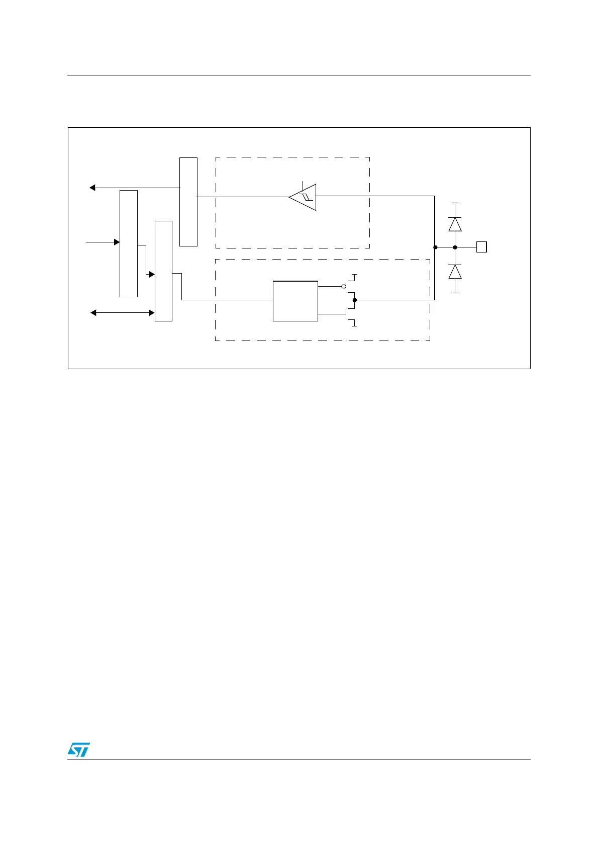
The Figure 16 on page 159 shows the Output configuration of the I/O Port bit.
Figure 16. Output configuration
1. V
DD_FT
is a potential specific to five-volt tolerant I/Os and different from V
DD
.
9.1.9 Alternate function configuration
When the I/O Port is programmed as Alternate Function:
● The Output Buffer is turned on in Open Drain or Push-Pull configuration
● The Output Buffer is driven by the signal coming from the peripheral (alternate function
out)
● The Schmitt Trigger Input is activated
● The weak pull-up and pull-down resistors are disabled.
● The data present on the I/O pin is sampled into the Input Data Register every APB2
clock cycle
● A read access to the Input Data Register gets the I/O state in open drain mode
● A read access to the Output Data register gets the last written value in Push-Pull mode
The Figure 17 on page 160 shows the Alternate Function Configuration of the I/O Port bit.
Also, refer to Section 9.4: AFIO registers on page 176 for further information.
A set of Alternate Function I/O registers allow you to remap some alternate functions to
different pins. Refer to
Push-pull or
Open-drain
Output
control
I/O pin
V
DD
V
SS
TTL Schmitt
trigger
V
SS
V
DD
or V
DD_FT
(1)
Protection
diode
Protection
diode
on
Input driver
Output driver
P-MOS
N-MOS
Input data register
Output data register
Read/write
Read
Bit set/reset registers
Write
ai14784
 Loading...


