Serial peripheral interface (SPI) RM0008
678/1096 Doc ID 13902 Rev 12
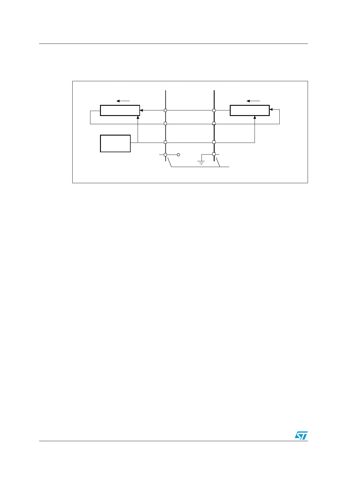
A basic example of interconnections between a single master and a single slave is
illustrated in Figure 237.
Figure 237. Single master/ single slave application
1. Here, the NSS pin is configured as an input.
The MOSI pins are connected together and the MISO pins are connected together. In this
way data is transferred serially between master and slave (most significant bit first).
The communication is always initiated by the master. When the master device transmits
data to a slave device via the MOSI pin, the slave device responds via the MISO pin. This
implies full-duplex communication with both data out and data in synchronized with the
same clock signal (which is provided by the master device via the SCK pin).
Slave select (NSS) pin management
There are two NSS modes:
● Software NSS mode: this mode is enabled by setting the SSM bit in the SPI_CR1
register (see Figure 238). In this mode, the external NSS pin is free for other
application uses and the internal NSS signal level is driven by writing to the SSI bit in
the SPI_CR1 register.
● Hardware NSS mode: there are two cases:
– NSS output is enabled: when the STM32F10xxx are operates as a Master and the
NSS output is enabled through the SSOE bit in the SPI_CR2 register, the NSS pin
is driven low and all the NSS pins of devices connected to the Master NSS pin see
a low level and become slaves when they are configured in NSS hardware mode.
When an SPI wants to broadcast a message, it has to pull NSS low to inform all
others that there is now a master for the bus. If it fails to pull NSS low, this means
that there is another master communicating, and a Hard Fault error occurs.
– NSS output is disabled: the multimaster capability is allowed.
8-bit shift register
SPI clock
generator
8-bit shift register
MISO
MOSI MOSI
MISO
SCK SCK
SlaveMaster
NSS
(1)
NSS
(1)
V
DD
MSBit LSBit MSBit LSBit
Not used if NSS is managed
by software
ai14745
 Loading...


