RM0008 Analog-to-digital converter (ADC)
Doc ID 13902 Rev 12 219/1096
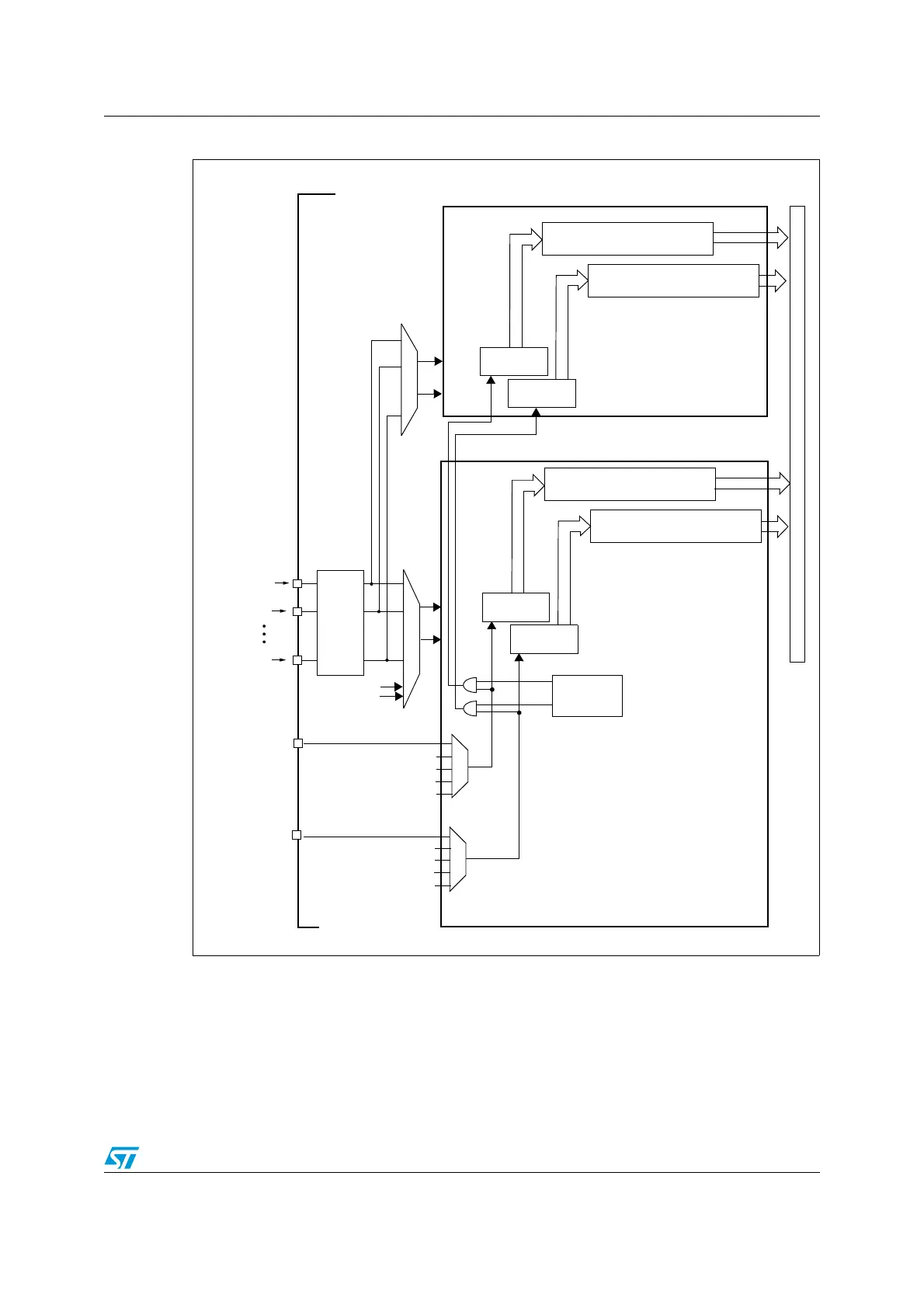
Figure 29. Dual ADC block diagram
(1)
1. External triggers are present on ADC2 but are not shown for the purposes of this diagram.
2. In some dual ADC modes, the ADC1 data register (ADC1_DR) contains both ADC1 and ADC2 regular converted data over
the entire 32 bits.
ADCx_IN0
ADCx_IN1
ADCx_IN15
GPIO
Ports
Address/data bus
EXTI_11
EXTI_15
Injected data registers
(4 x 16 bits)
Regular
channels
Injected
channels
ADC2 (Slave)
(12 bits)
Injected data registers
(4 x 16 bits)
Regular
channels
injected
channels
ADC1 (Master)
Dual mode
internal triggers
Start trigger mux
(regular group)
(injected group)
Start trigger mux
control
Temp. sensor
V
REFINT
Regular data register
(16 bits)
Regular data register
(16 bits)
(2)
 Loading...


