RM0008 Memory and bus architecture
Doc ID 13902 Rev 12 47/1096
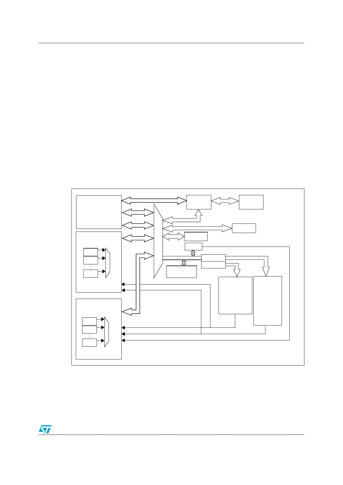
3 Memory and bus architecture
3.1 System architecture
In low-, medium-, high- and XL-density devices, the main system consists of:
● Four masters:
– Cortex™-M3 core DCode bus (D-bus) and System bus (S-bus)
– GP-DMA1 & 2 (general-purpose DMA)
● Four slaves:
– Internal SRAM
– Internal Flash memory
–FSMC
– AHB to APBx (APB1 or APB2), which connect all the APB peripherals
These are interconnected using a multilayer AHB bus architecture as shown in Figure 1:
Figure 1. System architecture
FLITF
Ch.1
Ch.2
Ch.7
Cortex-M3
DMA1
ICode
DCode
System
AHB system bus
DMA Request
APB1
Flash
Bridge 2
Bridge 1
Ch.1
Ch.2
Ch.5
DMA2
SRAM
FSMC
SDIO
APB2
DMA request
ADC3
GPIOC
USART1
TIM8
SPI1
TIM1
ADC2
ADC1
GPIOG
GPIOF
GPIOE
GPIOD
GPIOB
GPIOA
EXTI
AFIO
DAC SPI3/I2S
TIM2
PWR
BKP
bxCAN
USB
I2C2
I2C1
UART5
UART4
USART3
USART2
SPI2/I2S
IWDG
WWDG
RTC
TIM7
TIM6
TIM5
TIM4
TIM3
ai14800c
Bus matrix
DMA
DMA
Reset & clock
control (RCC)
 Loading...


