Universal serial bus full-speed device interface (USB) RM0008
604/1096 Doc ID 13902 Rev 12
clock is fixed by the requirements of the USB standard at 48 MHz, and this can be different
from the clock used for the interface to the APB1 bus. Different clock configurations are
possible where the APB1 clock frequency can be higher or lower than the USB peripheral
one.
Note: Due to USB data rate and packet memory interface requirements, the APB1 clock frequency
must be greater than 8 MHz to avoid data overrun/underrun problems.
Each endpoint is associated with two packet buffers (usually one for transmission and the
other one for reception). Buffers can be placed anywhere inside the packet memory
because their location and size is specified in a buffer description table, which is also
located in the packet memory at the address indicated by the USB_BTABLE register. Each
table entry is associated to an endpoint register and it is composed of four 16-bit words so
that table start address must always be aligned to an 8-byte boundary (the lowest three bits
of USB_BTABLE register are always “000”). Buffer descriptor table entries are described in
the Section 23.5.3: Buffer descriptor table. If an endpoint is unidirectional and it is neither an
Isochronous nor a double-buffered bulk, only one packet buffer is required (the one related
to the supported transfer direction). Other table locations related to unsupported transfer
directions or unused endpoints, are available to the user. Isochronous and double-buffered
bulk endpoints have special handling of packet buffers (Refer to Section 23.4.4: Isochronous
transfers and Section 23.4.3: Double-buffered endpoints respectively). The relationship
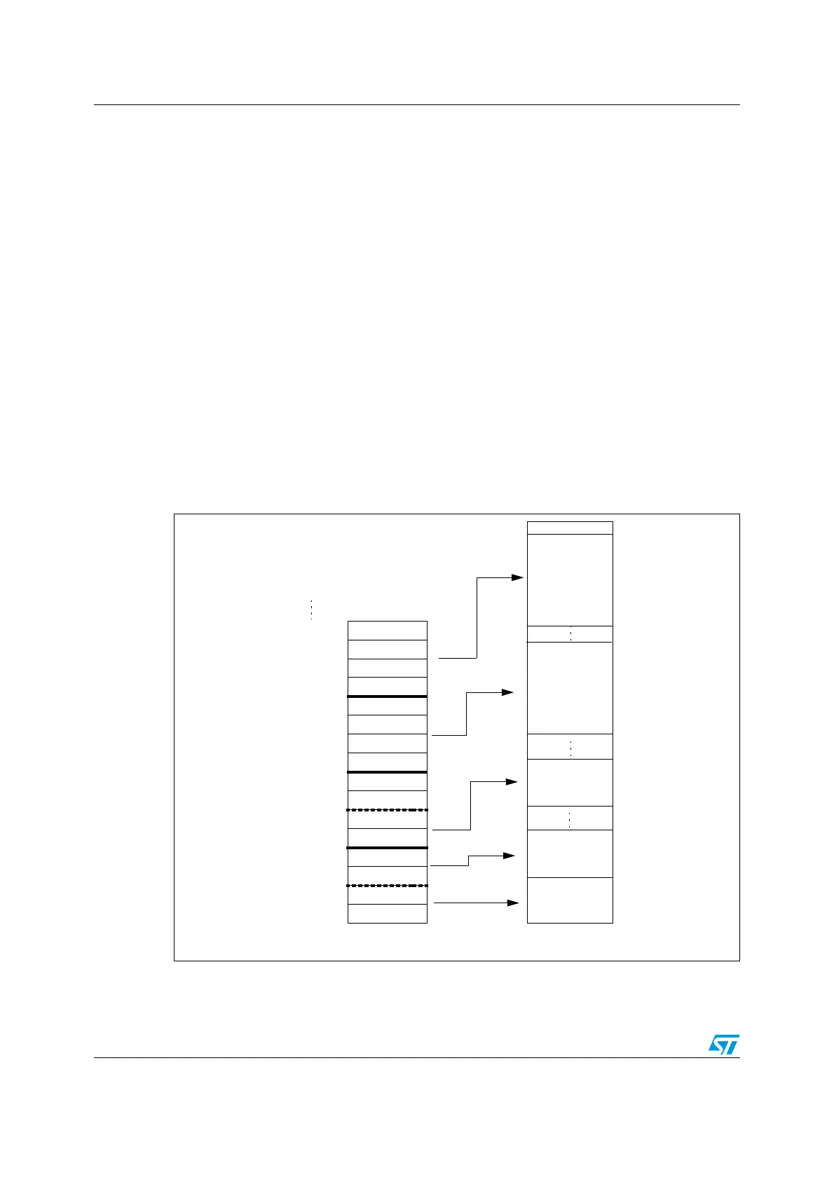
between buffer description table entries and packet buffer areas is depicted in Figure 220.
Figure 220. Packet buffer areas with examples of buffer description table locations
Buffer for
double-buffered
IN Endpoint 3
ADDR0_TX
COUNT0_TX
0000_0000 (00)
ADDR0_RX
COUNT0_RX
ADDR1_TX
COUNT1_TX
ADDR1_RX
COUNT1_RX
ADDR2_RX_0
COUNT2_RX_0
ADDR2_RX_1
COUNT2_RX_1
ADDR3_TX_0
COUNT3_TX_0
0000_0010 (02)
0000_0100 (04)
0000_0110 (06)
0000_1000 (08)
0000_1010 (0A)
0000_1100 (0C)
0000_1110 (0E)
0001_0000 (10)
0001_0010 (12)
0001_0100 (14)
0001_0110 (16)
0001_1000 (18)
0001_1010 (1A)
Buffer description table locations
Transmission
buffer for
Endpoint 0
Reception buffer
for
Endpoint 0
Transmission
buffer for
single-buffered
Endpoint 1
Packet buffers
ADDR3_TX_1
COUNT3_TX_1
0001_1100 (1C)
0001_1110 (1E)
Buffer for
double-buffered
OUT Endpoint 2
ai17109
 Loading...


