RM0008 Advanced-control timers (TIM1&TIM8)
Doc ID 13902 Rev 12 305/1096
14.3.11 Complementary outputs and dead-time insertion
The advanced-control timers (TIM1&TIM8) can output two complementary signals and
manage the switching-off and the switching-on instants of the outputs.
This time is generally known as dead-time and you have to adjust it depending on the
devices you have connected to the outputs and their characteristics (intrinsic delays of level-
shifters, delays due to power switches...)
You can select the polarity of the outputs (main output OCx or complementary OCxN)
independently for each output. This is done by writing to the CCxP and CCxNP bits in the
TIMx_CCER register.
The complementary signals OCx and OCxN are activated by a combination of several
control bits: the CCxE and CCxNE bits in the TIMx_CCER register and the MOE, OISx,
OISxN, OSSI and OSSR bits in the TIMx_BDTR and TIMx_CR2 registers. Refer to Ta ble 8 3 :
Output control bits for complementary OCx and OCxN channels with break feature on
page 337 for more details. In particular, the dead-time is activated when switching to the
IDLE state (MOE falling down to 0).
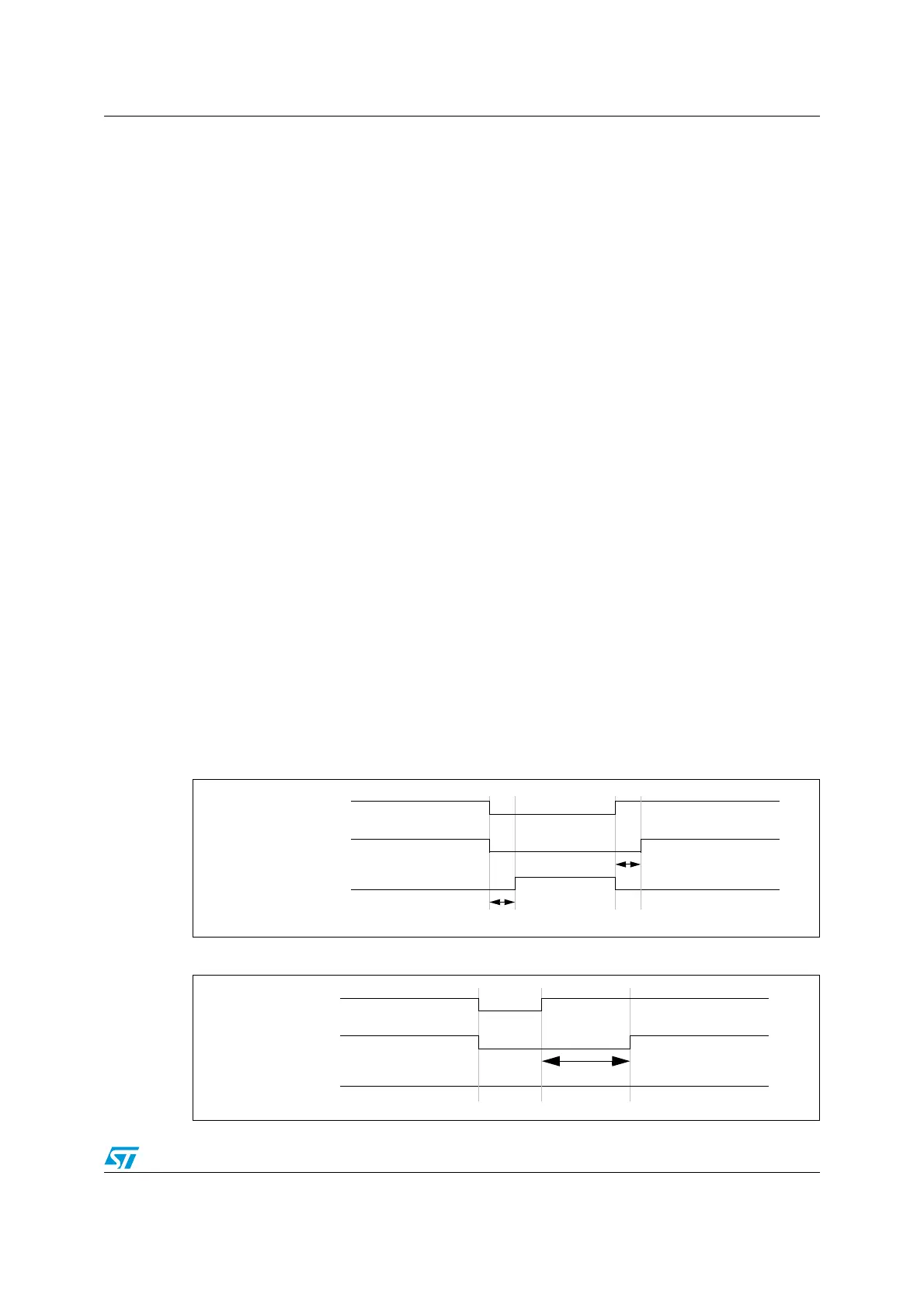
Dead-time insertion is enabled by setting both CCxE and CCxNE bits, and the MOE bit if the
break circuit is present. There is one 10-bit dead-time generator for each channel. From a
reference waveform OCxREF, it generates 2 outputs OCx and OCxN. If OCx and OCxN are
active high:
● The OCx output signal is the same as the reference signal except for the rising edge,
which is delayed relative to the reference rising edge.
● The OCxN output signal is the opposite of the reference signal except for the rising
edge, which is delayed relative to the reference falling edge.
If the delay is greater than the width of the active output (OCx or OCxN) then the
corresponding pulse is not generated.
The following figures show the relationships between the output signals of the dead-time
generator and the reference signal OCxREF. (we suppose CCxP=0, CCxNP=0, MOE=1,
CCxE=1 and CCxNE=1 in these examples)
Figure 86. Complementary output with dead-time insertion.
Figure 87. Dead-time waveforms with delay greater than the negative pulse.
 Loading...


