Advanced-control timers (TIM1&TIM8) RM0008
344/1096 Doc ID 13902 Rev 12
14.4.20 TIM1&TIM8 DMA address for full transfer (TIMx_DMAR)
Address offset: 0x4C
Reset value: 0x0000
14.4.21 TIM1&TIM8 register map
TIM1&TIM8 registers are mapped as 16-bit addressable registers as described in the table
below:
Bits 4:0 DBA[4:0]: DMA base address
This 5-bits vector defines the base-address for DMA transfers (when read/write access are
done through the TIMx_DMAR address). DBA is defined as an offset starting from the
address of the TIMx_CR1 register.
Example:
00000: TIMx_CR1,
00001: TIMx_CR2,
00010: TIMx_SMCR,
...
Example: Let us consider the following transfer: DBL = 7 bytes & DBA = TIMx_CR1. In this
case the transfer is done to/from 7 registers starting from the TIMx_CR1 address..
– If DBL = 7 bytes and DBA = TIM2_CR1 represents the address of the byte to be transferred,
the address of the transfer should be given by the following equation:
(TIMx_CR1 address) + DBA + (DMA index), where DMA index = DBL
In this example, 7 bytes are added to (TIMx_CR1 address) + DBA, which gives us the address
from/to which the data will be copied. In this case, the transfer is done to 7 registers starting
from the following address: (TIMx_CR1 address) + DBA
According to the configuration of the DMA Data Size, several cases may occur:
– If you configure the DMA Data Size in half-words, 16-bit data will be transferred to each of
the 7 registers.
If you configure the DMA Data Size in bytes, the data will aslo be transferred to 7 registers:
the first register will contain the first MSB byte, the second register, the first LSB byte and so
on. So with the transfer Timer, you also have to specify the size of data transferred by DMA.
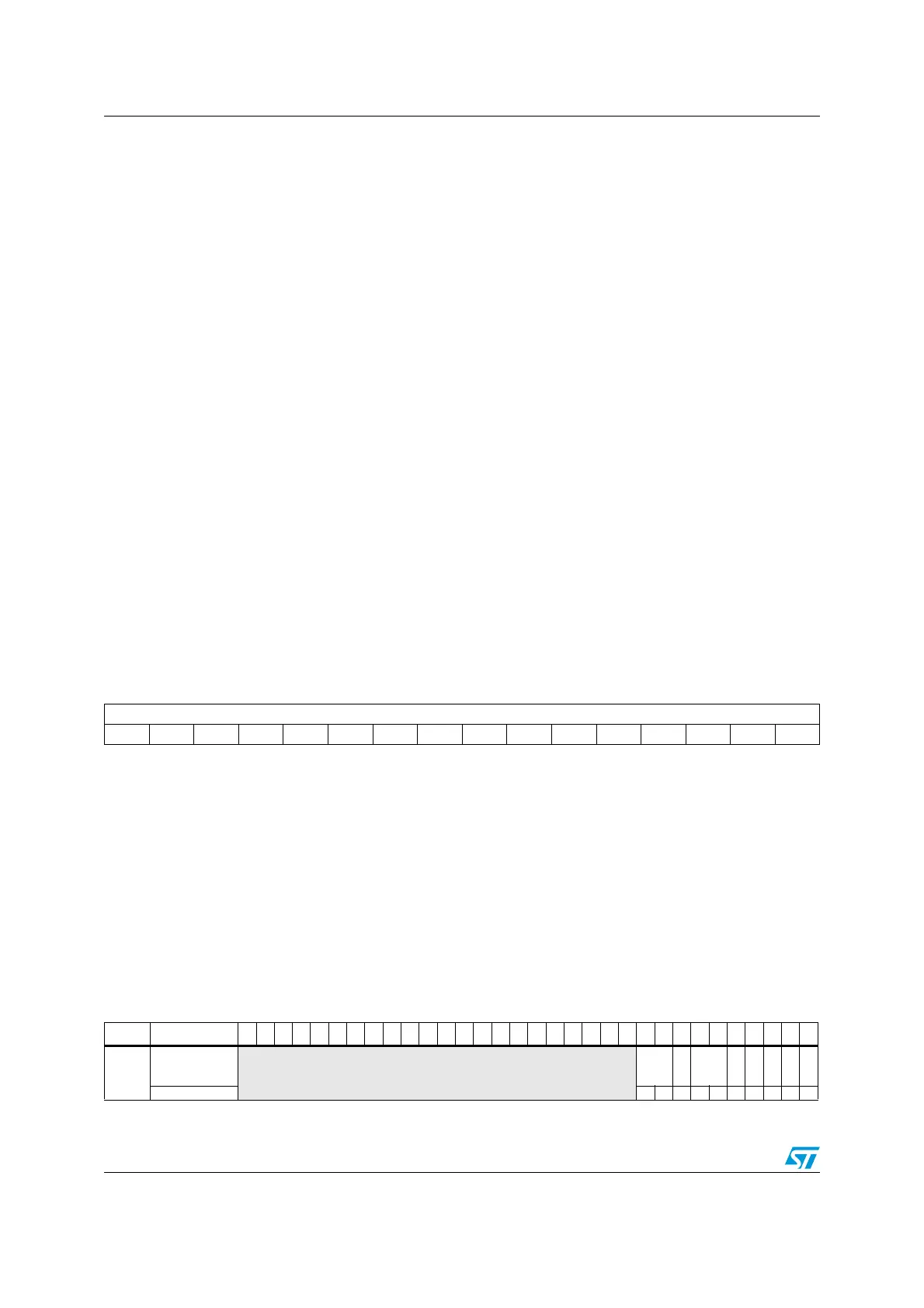
1514131211109876543210
DMAB[15:0]
rw rw rw rw rw rw rw rw rw rw rw rw rw rw rw rw
Bits 15:0 DMAB[15:0]: DMA register for burst accesses
A read or write access to the DMAR register accesses the register located at the address:
“(TIMx_CR1 address) + DBA + (DMA index)” in which:
TIMx_CR1 address is the address of the control register 1, DBA is the DMA base address
configured in TIMx_DCR register, DMA index is the offset automatically controlled by the
DMA transfer, depending on the length of the transfer DBL in the TIMx_DCR register.
Table 84. TIM1&TIM8 register map and reset values
Offset Register
31
30
29
28
27
26
25
24
23
22
21
20
19
18
17
16
15
14
13
12
11
10
9
8
7
6
5
4
3
2
1
0
0x00
TIMx_CR1
Reserved
CKD
[1:0]
ARPE
CMS
[1:0]
DIR
OPM
URS
UDIS
CEN
Reset value 0000000000
 Loading...


