Flexible static memory controller (FSMC) RM0008
492/1096 Doc ID 13902 Rev 12
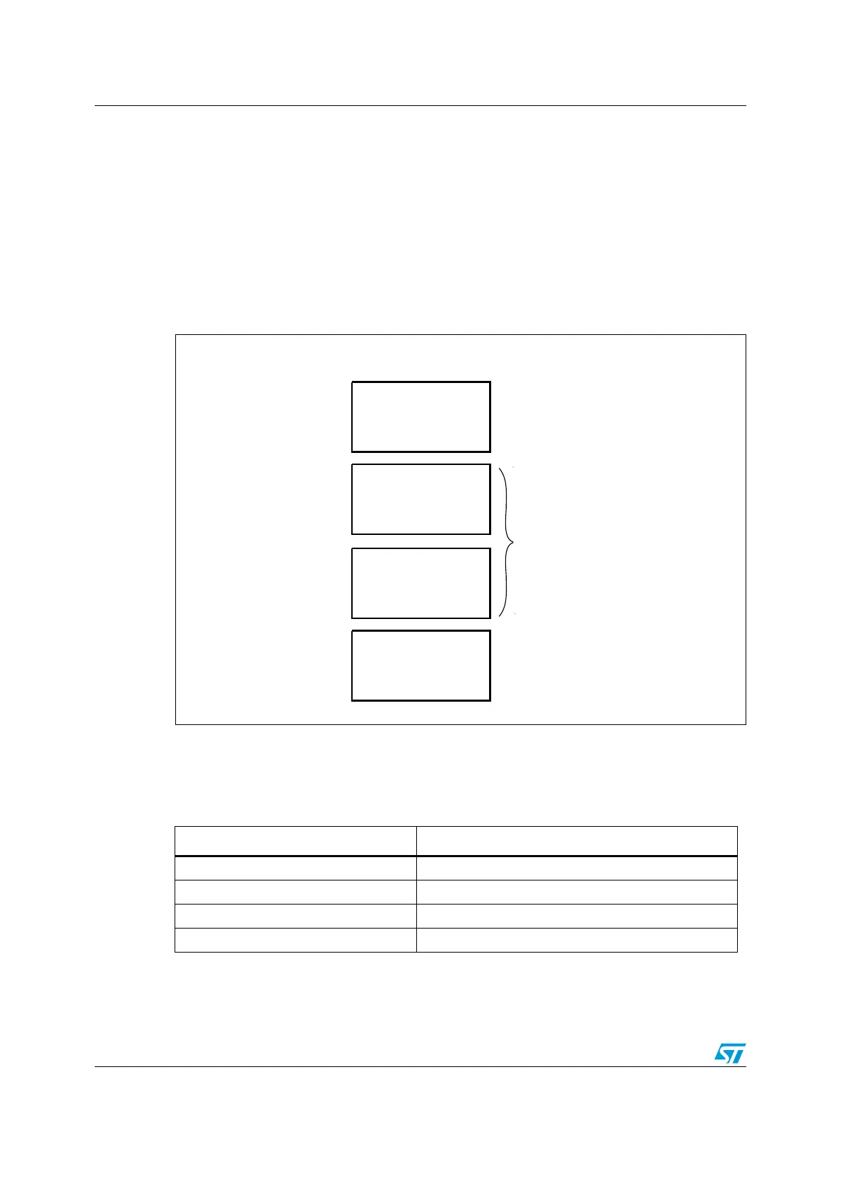
21.4 External device address mapping
From the FSMC point of view, the external memory is divided into 4 fixed-size banks of 256
Mbytes each (Refer to Figure 186):
● Bank 1 used to address up to 4 NOR Flash or PSRAM memory devices. This bank is
split into 4 NOR/PSRAM regions with 4 dedicated Chip Select.
● Banks 2 and 3 used to address NAND Flash devices (1 device per bank)
● Bank 4 used to address a PC Card device
For each bank the type of memory to be used is user-defined in the Configuration register.
Figure 186. FSMC memory banks
21.4.1 NOR/PSRAM address mapping
HADDR[27:26] bits are used to select one of the four memory banks as shown in Tabl e 9 9.
Bank 1
NAND Flash
NOR / PSRAM
Supported memory typeBanks
4 × 64 MB
6000 0000h
6FF F FFF Fh
Address
7000 0000h
7FF F FFF Fh
8000 0000h
8FF F FFF Fh
9000 0000h
9FF F FFF Fh
Bank 2
4 × 64 MB
Bank 3
4 × 64 MB
Bank 4
4 × 64 MB
PC Card
ai14719
Table 99. NOR/PSRAM bank selection
HADDR[27:26]
(1)
1. HADDR are internal AHB address lines that are translated to external memory.
Selected bank
00 Bank 1 NOR/PSRAM 1
01 Bank 1 NOR/PSRAM 2
10 Bank 1 NOR/PSRAM 3
11 Bank 1 NOR/PSRAM 4
 Loading...


