RM0008 Flexible static memory controller (FSMC)
Doc ID 13902 Rev 12 535/1096
21.6.8 NAND Flash/PC Card controller registers
The peripheral registers have to be accessed by words (32-bit).
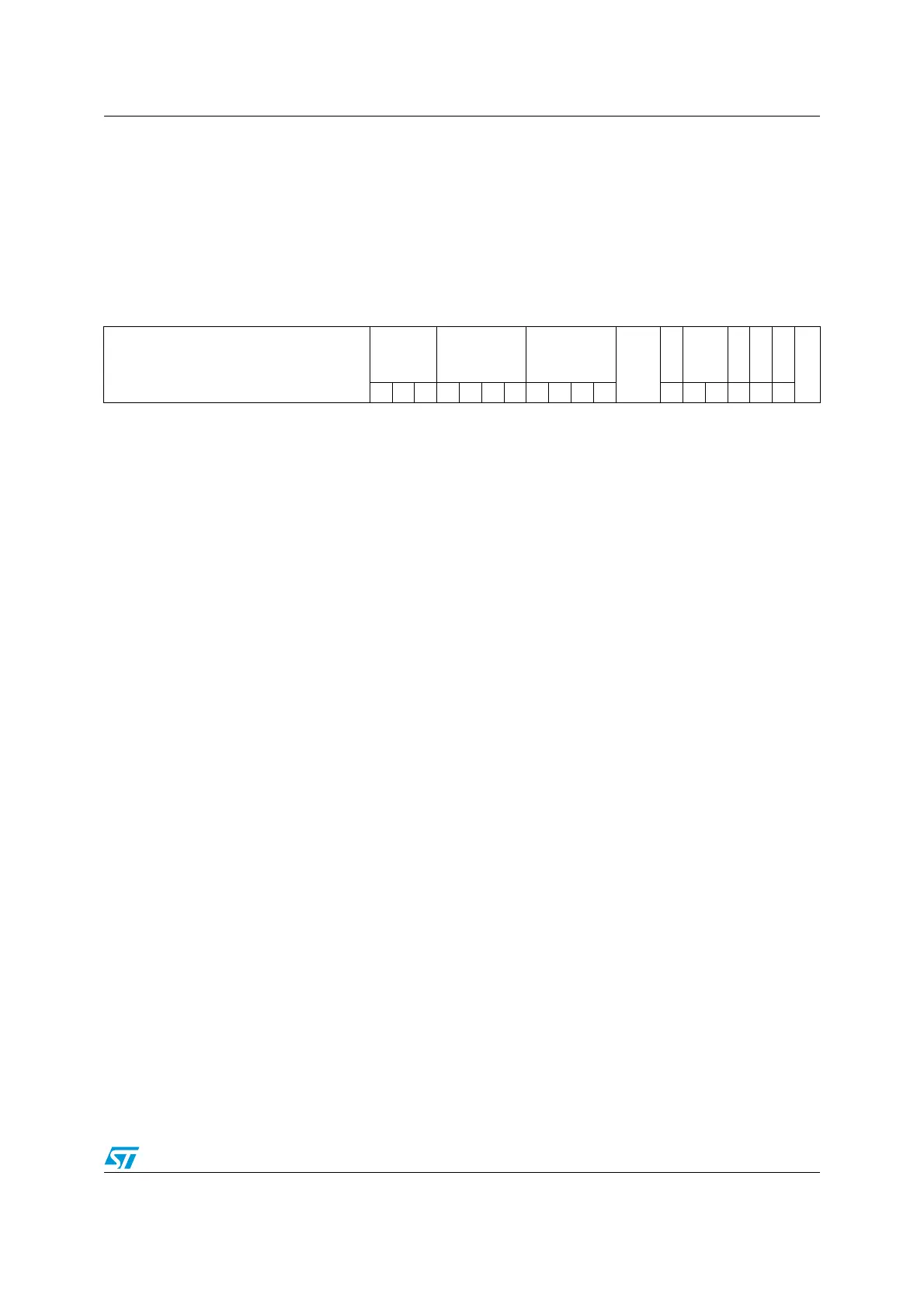
PC Card/NAND Flash control registers 2..4 (FSMC_PCR2..4)
Address offset: 0xA0000000 + 0x40 + 0x20 * (x – 1), x = 2..4
Reset value: 0x0000 0018
31302928272625242322212019181716151413121110987654321 0
Reserved
ECCPS TAR TCLR
Res.
ECCEN
PWID
PTYP
PBKEN
PWAITEN
Reserved
rw rw rw rw rw rw rw rw rw rw rw rw rw rw rw rw rw
Bits 19:17 ECCPS: ECC page size.
Defines the page size for the extended ECC:
000: 256 bytes
001: 512 bytes
010: 1024 bytes
011: 2048 bytes
100: 4096 bytes
101: 8192 bytes
Bits 16:13 TAR: ALE to RE delay.
Sets time from ALE low to RE low in number of AHB clock cycles (HCLK).
Time is: t_ar = (TAR + SET + 4) × THCLK where THCLK is the HCLK clock period
0000: 1 HCLK cycle (default)
1111: 16 HCLK cycles
Note: SET is MEMSET or ATTSET according to the addressed space.
Bits 12:9 TCLR: CLE to RE delay.
Sets time from CLE low to RE low in number of AHB clock cycles (HCLK).
Time is t_clr = (TCLR + SET + 4) × THCLK where THCLK is the HCLK clock period
0000: 1 HCLK cycle (default)
1111: 16 HCLK cycles
Note: SET is MEMSET or ATTSET according to the addressed space.
Bits 8:7 Reserved.
Bits 6 ECCEN: ECC computation logic enable bit
0: ECC logic is disabled and reset (default after reset),
1: ECC logic is enabled.
Bits 5:4 PWID: Databus width.
Defines the external memory device width.
00: 8 bits (default after reset)
01: 16 bits (mandatory for PC Card)
10: reserved, do not use
11: reserved, do not use
Bit 3 PTYP: Memory type.
Defines the type of device attached to the corresponding memory bank:
0: PC Card, CompactFlash, CF+ or PCMCIA
1: NAND Flash (default after reset)
 Loading...


