Flexible static memory controller (FSMC) RM0008
534/1096 Doc ID 13902 Rev 12
The FSMC Bank 4 gives access to those 3 memory spaces as described in Section 21.4.2:
NAND/PC Card address mapping - Table 101: Memory mapping and timing registers
Wait Feature
The CompactFlash Storage or PC Card may request the FSMC to extend the length of the
access phase programmed by MEMWAITx/ATTWAITx/IOWAITx bits, asserting the nWAIT
signal after nOE/nWE or nIORD/nIOWR activation if the wait feature is enabled through the
PWAITEN bit in the FSMC_PCRx register. In order to detect the nWAIT assertion correctly,
the MEMWAITx/ATTWAITx/IOWAITx bits must be programmed as follows:
xxWAITx >= 4 + max_wait_assertion_time/HCLK
Where max_wait_assertion_time is the maximum time taken by NWAIT to go low once
nOE/nWE or nIORD/nIOWR is low.
After the de-assertion of nWAIT, the FSMC extends the WAIT phase for 4 HCLK clock
cycles.
1 0 010XXX-X0
I/O space
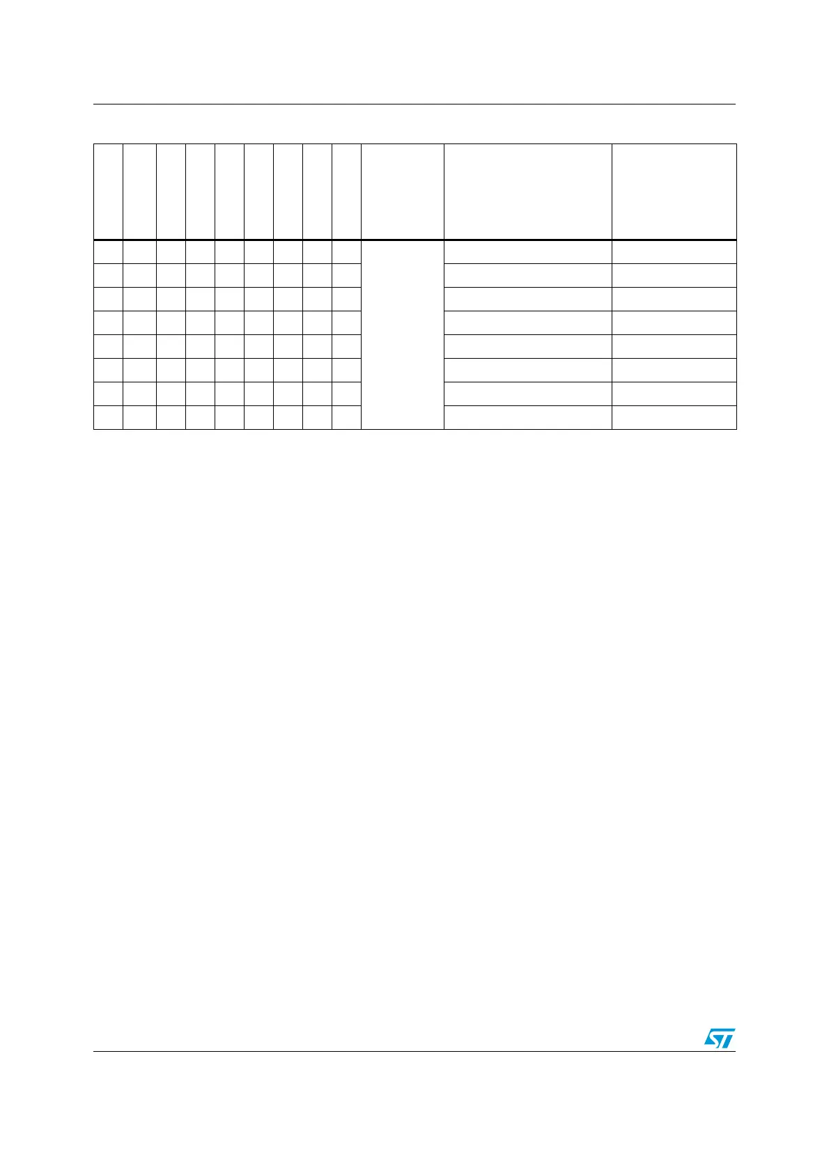
Read Even Byte on D7-0 Not supported
1 0 0 1 0 X X X-X 1 Read Odd Byte on D7-0 Not supported
1 0 0 1 0 X X X-X 0 Write Even Byte on D7-0 Not supported
1 0 0 1 0 X X X-X 1 Write Odd Byte on D7-0 Not supported
0 0 0 1 0 X X X-X 0 Read Word on D15-0 YES
0 0 0 1 0 X X X-X 0 Write word on D15-0 YES
0 1 0 1 0 X X X-X X Read Odd Byte on D15-8 Not supported
0 1 0 1 0 X X X-X X Write Odd Byte on D15-8 Not supported
Table 133. 16-bit PC-Card signals and access type (continued)
nCE2
nCE1
nREG
nOE/nWE
nIORD /nIOWR
A10
A9
A7-1
A0
Space Access Type
Allowed/not
Allowed
 Loading...


