USB on-the-go full-speed (OTG_FS) RM0008
934/1096 Doc ID 13902 Rev 12
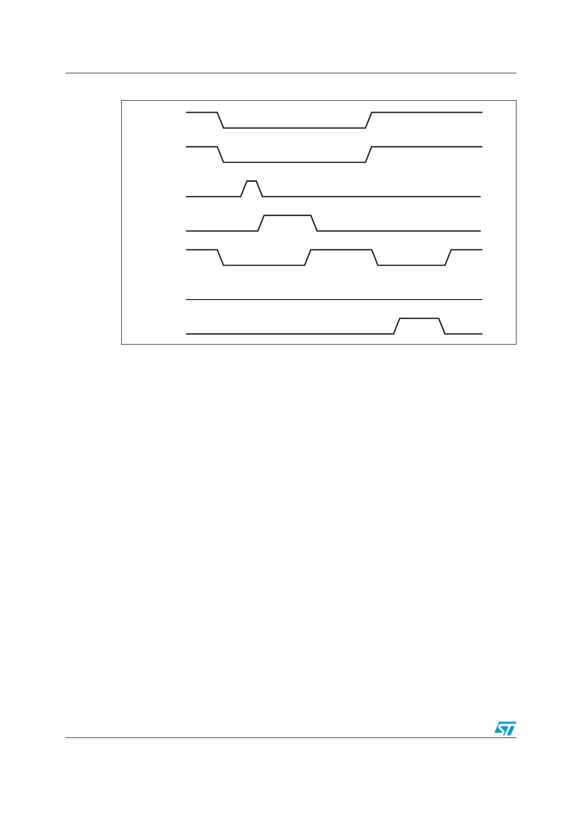
Figure 322. B-device SRP
1. VBUS_VALID = V
BUS
valid signal from PHY
B_VALID = B-peripheral valid session to PHY
DISCHRG_VBUS = discharge signal to PHY
SESS_END = session end signal to PHY
CHRG_VBUS = charge V
BUS
signal to PHY
DP = Data plus line
DM = Data minus line
1. To save power, the host suspends and turns off port power when the bus is idle.
The OTG_FS controller sets the early suspend bit in the Core interrupt register after 3
ms of bus idleness. Following this, the OTG_FS controller sets the USB suspend bit in
the Core interrupt register.
The OTG_FS controller informs the PHY to discharge V
BUS
.
2. The PHY indicates the session’s end to the device. This is the initial condition for SRP.
The OTG_FS controller requires 2 ms of SE0 before initiating SRP.
For a USB 1.1 full-speed serial transceiver, the application must wait until V
BUS
discharges to 0.2 V after BSVLD (in OTG_FS_GOTGCTL) is deasserted. This
discharge time can be obtained from the transceiver vendor and varies from one
transceiver to another.
3. The application initiates SRP by writing the session request bit in the OTG Control and
status register. The OTG_FS controller perform data-line pulsing followed by V
BUS
pulsing.
4. The host detects SRP from either the data-line or V
BUS
pulsing, and turns on V
BUS
.
The PHY indicates V
BUS
power-on to the device.
5. The OTG_FS controller performs V
BUS
pulsing.
The host starts a new session by turning on V
BUS
, indicating SRP success. The
OTG_FS controller interrupts the application by setting the session request success
status change bit in the OTG interrupt status register. The application reads the session
request success bit in the OTG control and status register.
6. When the USB is powered, the OTG_FS controller connects, completing the SRP
process.
ai15682
VBUS_VALID
B_VALID
DISCHRG_VBUS
SESS_END
DP
DM
CHRG_VBUS
Suspend
Data line pulsing Connect
V
BUS
pulsing
1
6
2
3
4
5 8
7
Low
 Loading...


