Flexible static memory controller (FSMC) RM0008
494/1096 Doc ID 13902 Rev 12
The application software uses the 3 sections to access the NAND Flash memory:
● To send a command to NAND Flash memory: the software must write the command
value to any memory location in the command section.
● To specify the NAND Flash address that must be read or written: the software must
write the address value to any memory location in the address section. Since an
address can be 4 or 5 bytes long (depending on the actual memory size), several
consecutive writes to the address section are needed to specify the full address.
● To read or write data: the software reads or writes the data value from or to any
memory location in the data section.
Since the NAND Flash memory automatically increments addresses, there is no need to
increment the address of the data section to access consecutive memory locations.
21.5 NOR Flash/PSRAM controller
The FSMC generates the appropriate signal timings to drive the following types of
memories:
● Asynchronous SRAM and ROM
–8-bit
– 16-bit
– 32-bit
● PSRAM (Cellular RAM)
– Asynchronous mode
– Burst mode
● NOR Flash
– Asynchronous mode or burst mode
– Multiplexed or nonmultiplexed
The FSMC outputs a unique chip select signal NE[4:1] per bank. All the other signals
(addresses, data and control) are shared.
For synchronous accesses, the FSMC issues the clock (CLK) to the selected external
device. This clock is a submultiple of the HCLK clock. The size of each bank is fixed and
equal to 64 Mbytes.
Each bank is configured by means of dedicated registers (see Section 21.5.6).
The programmable memory parameters include access timings (see Tab l e 1 0 3) and support
for wait management (for PSRAM and NOR Flash accessed in burst mode).
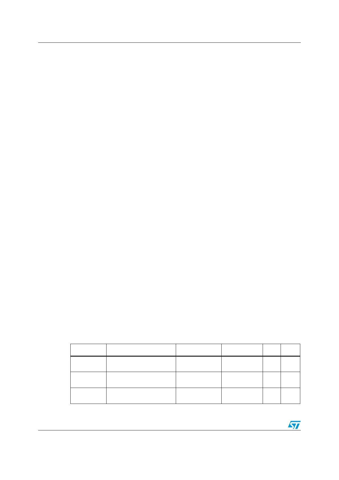
Table 103. Programmable NOR/PSRAM access parameters
Parameter Function Access mode Unit Min. Max.
Address
setup
Duration of the address
setup phase
Asynchronous
AHB clock cycle
(HCLK)
116
Address hold
Duration of the address hold
phase
Asynchronous,
muxed I/Os
AHB clock cycle
(HCLK)
216
Data setup
Duration of the data setup
phase
Asynchronous
AHB clock cycle
(HCLK)
2 256
 Loading...


