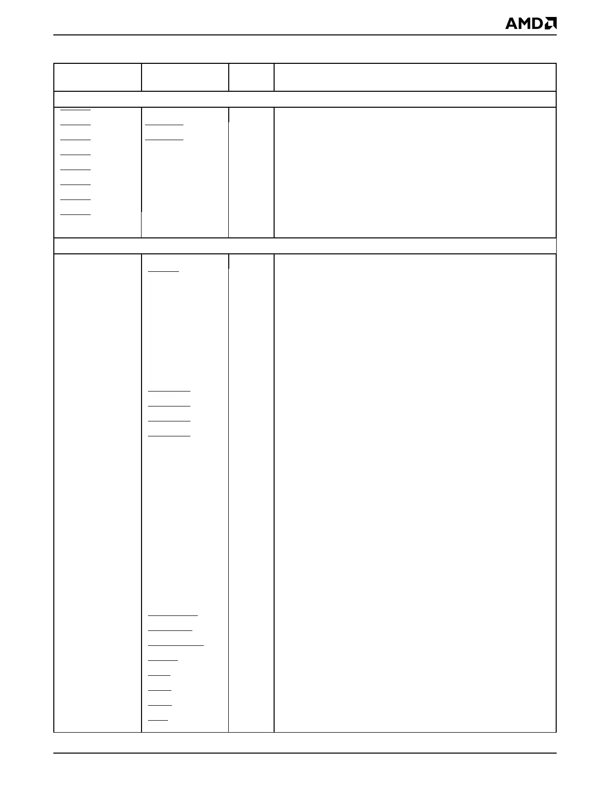
Pin Information
Élan™SC520 Microcontroller User’s Manual 2-11
Chip Selects
[GPCS0]PIO27 OGeneral-Purpose Chip Select signals are for the GP bus. They can
be used for either memory or I/O accesses. These chip selects are
asserted for Am5
x
86 CPU accesses to the corresponding regions set
up in the Programmable Address Region (PAR) registers.
[GPCS1
]ROMCS1 O
[GPCS2
]ROMCS2 O
[GPCS3
] PITGATE2 O
[GPCS4
]TMRIN1 O
[GPCS5
]TMRIN0 O
[GPCS6
]TMROUT1 O
[GPCS7
]TMROUT0 O
Programmable I/O (PIO)
PIO0 [GPALE] B Programmable Input/Output signals can be programmed as inputs
or outputs. When they are outputs, they can be driven High or Low by
programming bits in registers.
PIO1 [GPBHE
]B
PIO2 [GPRDY] B
PIO3 [GPAEN] B
PIO4 [GPTC] B
PIO5 [GPDRQ3] B
PIO6 [GPDRQ2] B
PIO7 [GPDRQ1] B
PIO8 [GPDRQ0] B
PIO9 [GPDACK3
]B
PIO10 [GPDACK2
]B
PIO11 [GPDACK1
]B
PIO12 [GPDACK0
]B
PIO13 [GPIRQ10] B
PIO14 [GPIRQ9] B
PIO15 [GPIRQ8] B
PIO16 [GPIRQ7] B
PIO17 [GPIRQ6] B
PIO18 [GPIRQ5] B
PIO19 [GPIRQ4] B
PIO20 [GPIRQ3] B
PIO21 [GPIRQ2] B
PIO22 [GPIRQ1] B
PIO23 [GPIRQ0] B
PIO24 [GPDBUFOE
]B
PIO25 [GPIOCS16
]B
PIO26 [GPMEMCS16
]B
PIO27 [GPCS0
]B
PIO28 [CTS2
]B
PIO29 [DSR2
]B
PIO30 [DCD2
]B
PIO31 [RIN2
]B
Table 2-2 Signal Descriptions (Continued)
Signal
Multiplexed
Signal Type Description