Pin Information
Élan™SC520 Microcontroller User’s Manual 2-13
[WBMSTR0] CF_ROM_GPCS
{CFG0}
O Write Buffer Master indicates which block(s) wrote to a rank in the
write buffer (during SDRAM write cycles) and which block is reading
from SDRAM (during SDRAM read cycles).
WBMSTR0, when a logical 1, indicates that the internal GP bus DMA
controller has contributed to the write buffer rank (write cycles) or is
reading from SDRAM (read cycles).
[WBMSTR1] DATASTRB
{CFG1}
O WBMSTR1, when a logical 1, indicates that the PCI master has
contributed to the write buffer rank (write cycles) or is reading from
SDRAM (read cycles).
[WBMSTR2] CF_DRAM
{CFG2}
O WBMSTR2, when a logical 1, it indicates that the CPU has contributed
to the write buffer rank (write cycles) or is reading from SDRAM (read
cycles).
Configuration
{AMDEBUG_DIS} GPA23 I AMDebug Disable is an active High configuration signal latched at the
assertion of Power Good (PWRGOOD). This pin has a built-in
pulldown resistor.
At Power Good assertion:
Low = Normal operation, mode can be enabled by software.
High = AMDebug mode is disabled and cannot be enabled by software.
{CFG0} CF_ROM_GPCS
[WBMSTR0]
I Configuration Inputs 3–0 are latched into the chip when PWRGOOD
is asserted. These signals are all shared with other features. These
signals have built-in pulldown resistors.
CFG0: Choose 8-, 16-, or 32-bit ROM/Flash interface for BOOTCS.
{CFG1} DATASTRB
[WBMSTR1]
I CFG1: Choose 8-, 16-, or 32-bit ROM/Flash interface for BOOTCS
.
{CFG2} CF_DRAM
[WBMSTR2]
I CFG2: When Low when PWRGOOD is asserted, the ÉlanSC520
microcontroller uses the GP data bus for BOOTCS. When seen as
High during PWRGOOD assertion, the BOOTCS
access is across the
SDRAM data bus. Default is Low (by a built-in pulldown resistor).
{CFG3} PITOUT2 I CFG3 (Internal AMD test mode enable):
For normal ÉlanSC520
microcontroller operation, do not pull High during reset.
{DEBUG_ENTER} GPA25 I Enter AMDebug Mode is an active High configuration signal latched
at the assertion of Power Good (PWRGOOD). This pin enables the
AMDebug mode, which causes the processor to fetch and execute
one instruction from the BOOTCS
device, and then enter AMDebug
mode where the CPU waits for debug commands to be delivered by
the JTAG port. This pin has a built-in pulldown resistor.
At PWRGOOD assertion:
High = AMDebug mode enabled
Low = Normal operation
{INST_TRCE} GPA24 I Instruction Trace is an active High configuration signal latched at the
assertion of Power Good (PWRGOOD). Enables trace record
generation from Power Good assertion. This pin has a built-in
pulldown resistor.
At PWRGOOD assertion:
High = Trace controller enabled to output trace records
Low = Normal operation
Table 2-2 Signal Descriptions (Continued)
Signal
Multiplexed
Signal Type Description
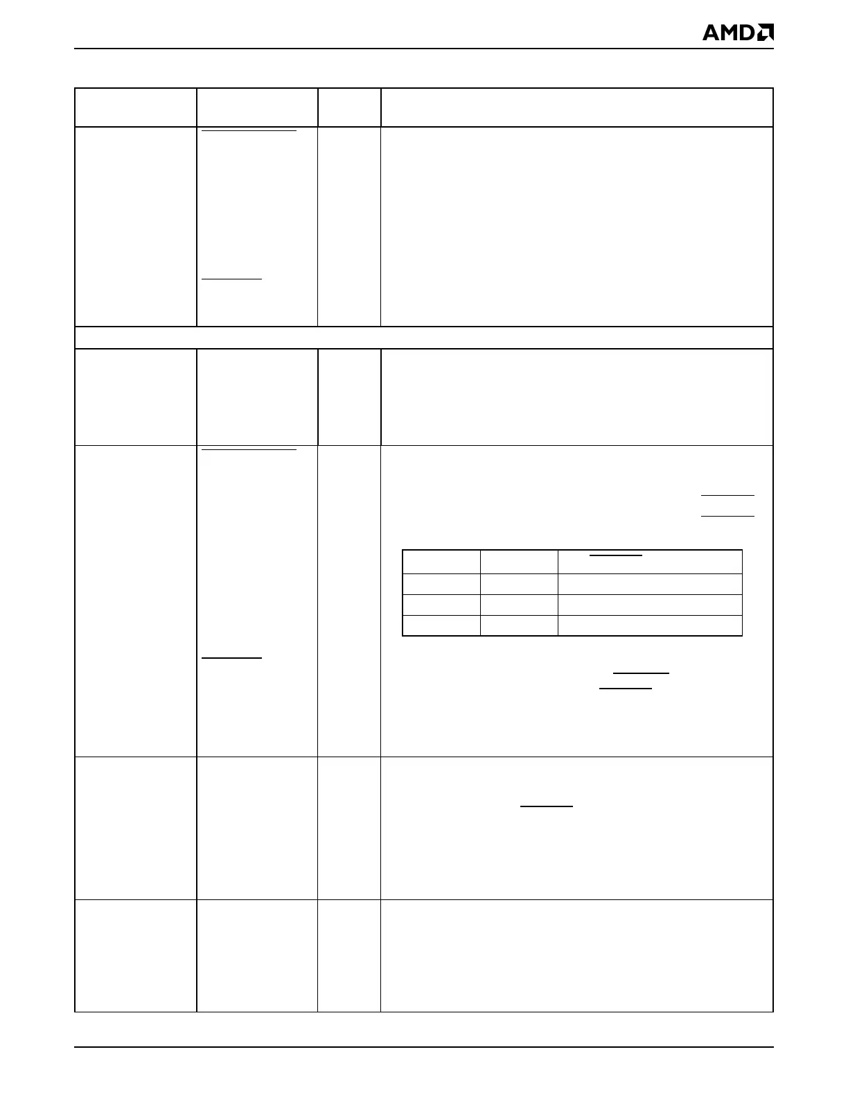
CFG1 CFG0 BOOTCS Data Width
00 8-bit
0 1 16-bit
1 x (don’t care) 32-bit