RM0008 DMA controller (DMA)
Doc ID 13902 Rev 12 279/1096
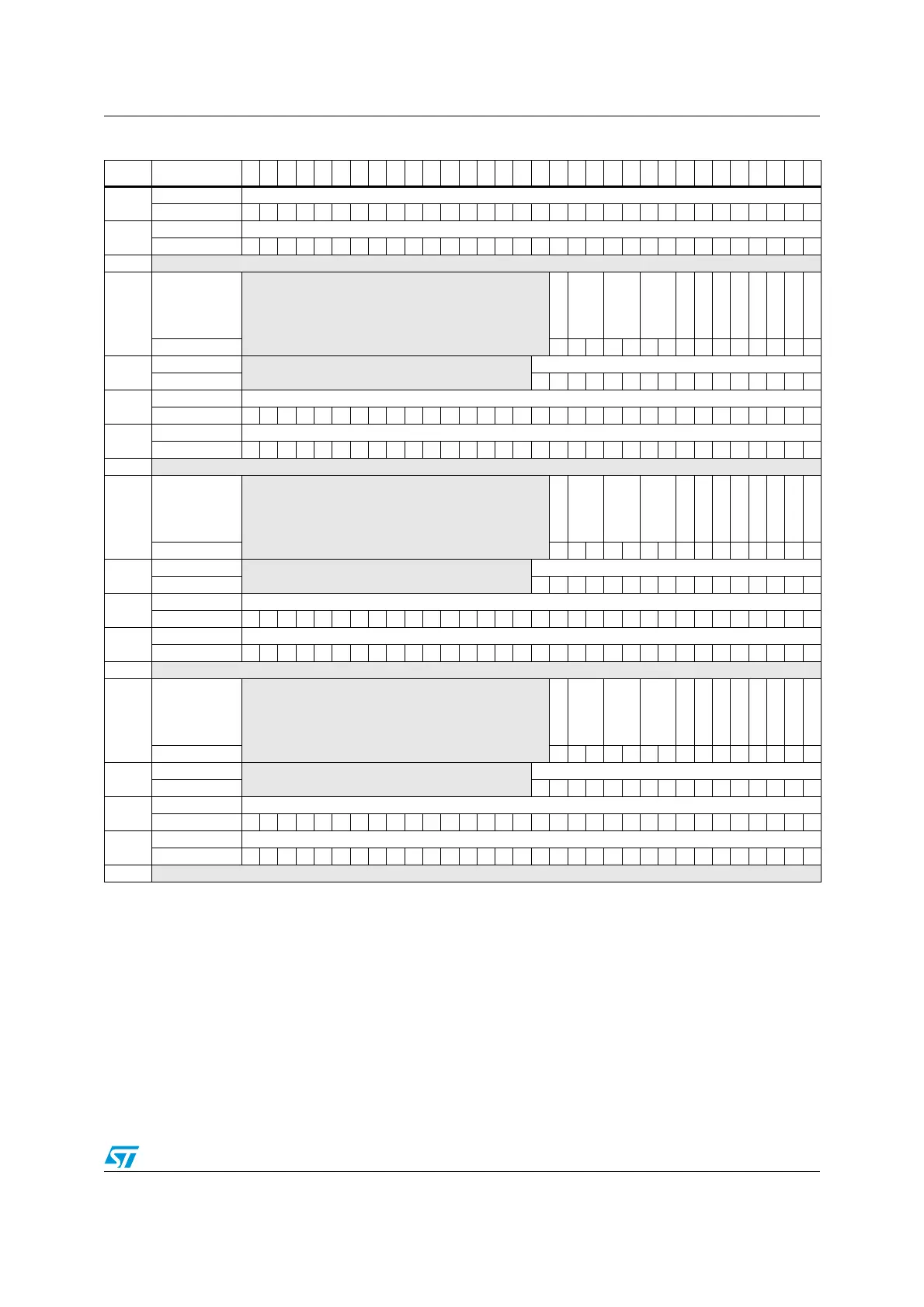
Refer to Table 3 on page 50 for the register boundary addresses.
0x04C
DMA_CPAR4 PA[31:0]
Reset value 00000000000000000000000000000000
0x050
DMA_CMAR4 MA[31:0]
Reset value 00000000000000000000000000000000
0x054
Reserved
0x058
DMA_CCR5
Reserved
MEM2MEM
PL
[1:0]
M SIZE [1:0]
PSIZE [1:0]
MINC
PINC
CIRC
DIR
TEIE
HTIE
TCIE
EN
Reset value 000000000000000
0x05C
DMA_CNDTR5
Reserved
NDT[15:0]
Reset value 0000000000000000
0x060
DMA_CPAR5 PA[31:0]
Reset value 00000000000000000000000000000000
0x064
DMA_CMAR5 MA[31:0]
Reset value 00000000000000000000000000000000
0x068
Reserved
0x06C
DMA_CCR6
Reserved
MEM2MEM
PL
[1:0]
M SIZE [1:0]
PSIZE [1:0]
MINC
PINC
CIRC
DIR
TEIE
HTIE
TCIE
EN
Reset value 000000000000000
0x070
DMA_CNDTR6
Reserved
NDT[15:0]
Reset value 0000000000000000
0x074
DMA_CPAR6 PA[31:0]
Reset value 00000000000000000000000000000000
0x078
DMA_CMAR6 MA[31:0]
Reset value 00000000000000000000000000000000
0x07C
Reserved
0x080
DMA_CCR7
Reserved
MEM2MEM
PL
[1:0]
M SIZE [1:0]
PSIZE [1:0]
MINC
PINC
CIRC
DIR
TEIE
HTIE
TCIE
EN
Reset value 000000000000000
0x084
DMA_CNDTR7
Reserved
NDT[15:0]
Reset value 0000000000000000
0x088
DMA_CPAR7 PA[31:0]
Reset value 00000000000000000000000000000000
0x08C
DMA_CMAR7 MA[31:0]
Reset value 00000000000000000000000000000000
0x090
Reserved
Table 80. DMA register map and reset values (continued)
Offset Register
31
30
29
28
27
26
25
24
23
22
21
20
19
18
17
16
15
14
13
12
11
10
9
8
7
6
5
4
3
2
1
0
 Loading...


