Flexible static memory controller (FSMC) RM0008
528/1096 Doc ID 13902 Rev 12
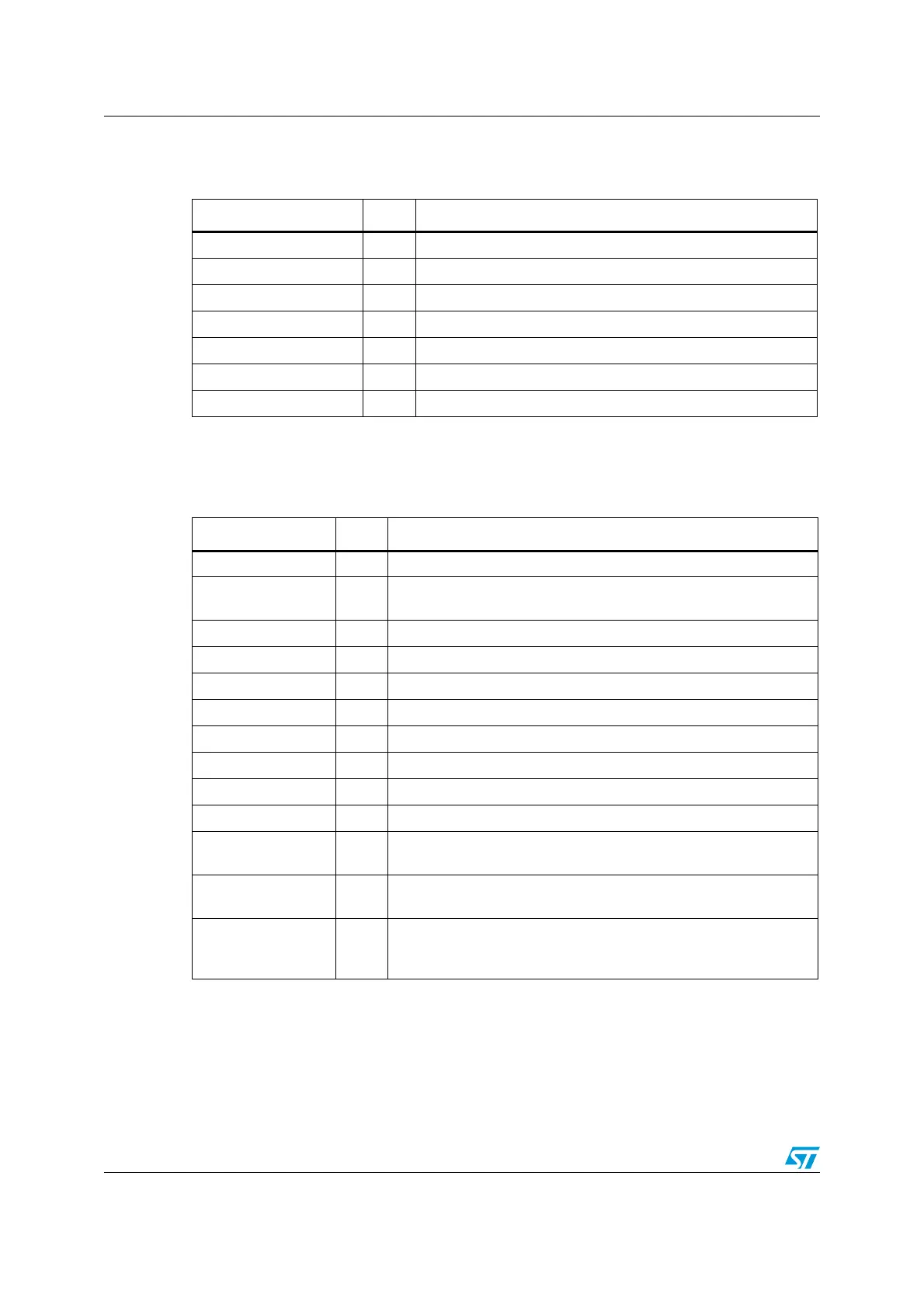
16-bit NAND Flash
There is no theoretical capacity limitation as the FSMC can manage as many address
cycles as needed.
Table 130. 16-bit NAND Flash
FSMC signal name I/O Function
A[17] O NAND Flash address latch enable (ALE) signal
A[16] O NAND Flash command latch enable (CLE) signal
D[15:0] I/O 16-bit multiplexed, bidirectional address/data bus
NCE[x] O Chip select, x = 2, 3
NOE(= NRE) O Output enable (memory signal name: read enable, NRE)
NWE O Write enable
NWAIT/INT[3:2] I NAND Flash ready/busy input signal to the FSMC
Table 131. 16-bit PC Card
FSMC signal name I/O Function
A[10:0] O Address bus
NIOS16 I
Data transfer in I/O space. It must be shorted to GND (16-bit tranfer
only)
NIORD O Output enable for I/O space
NIOWR O Write enable for I/O space
NREG O Register signal indicating if access is in Common or Attribute space
D[15:0] I/O Bidirectional databus
NCE4_1 O Chip select 1
NCE4_2 O Chip select 2 (indicates if access is 16-bit or 8-bit)
NOE O Output enable in Common and in Attribute space
NWE O Write enable in Common and in Attribute space
NWAIT I
PC Card wait input signal to the FSMC (memory signal name
IORDY)
INTR I
PC Card interrupt to the FSMC (only for PC Cards that can generate
an interrupt)
CD I
PC Card presence detection. Active high. If an access is performed
to the PC Card banks while CD is low, an AHB error is generated.
Refer to Section 21.3: AHB interface
 Loading...


