RM0090 Rev 18 1023/1749
RM0090 Secure digital input/output interface (SDIO)
1075
31.3.1 SDIO adapter
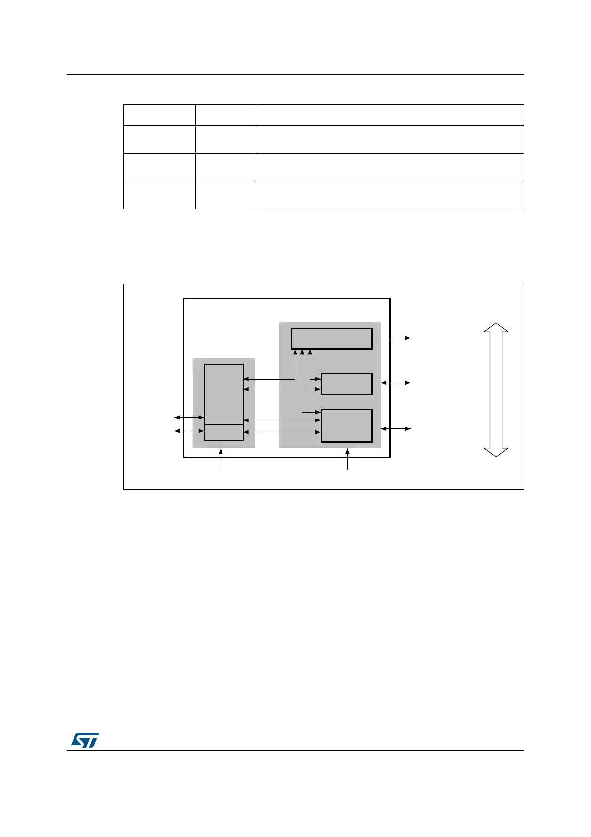
Figure 327 shows a simplified block diagram of an SDIO adapter.
Figure 327. SDIO adapter
The SDIO adapter is a multimedia/secure digital memory card bus master that provides an
interface to a multimedia card stack or to a secure digital memory card. It consists of five
subunits:
• Adapter register block
• Control unit
• Command path
• Data path
• Data FIFO
Note: The adapter registers and FIFO use the APB2 bus clock domain (PCLK2). The control unit,
command path and data path use the SDIO adapter clock domain (SDIOCLK).
Adapter register block
The adapter register block contains all system registers. This block also generates the
signals that clear the static flags in the multimedia card. The clear signals are generated
when 1 is written into the corresponding bit location in the SDIO Clear register.
Table 150. SDIO I/O definitions
Pin Direction Description
SDIO_CK Output
MultiMediaCard/SD/SDIO card clock. This pin is the clock from
host to card.
SDIO_CMD Bidirectional
MultiMediaCard/SD/SDIO card command. This pin is the
bidirectional command/response signal.
SDIO_D[7:0] Bidirectional
MultiMediaCard/SD/SDIO card data. These pins are the
bidirectional databus.
ai15899b
To APB2
interface
Control unit
Command
path
Data path
Adapter
registers
SDMMC_CK
SDMMC_CMD
SDMMC_D[7:0]
SDMMC adapter
PCLK2 SDMMCCLK
FIFO
Card bus