Serial peripheral interface (SPI) RM0090
876/1749 RM0090 Rev 18
28.3 SPI functional description
28.3.1 General description
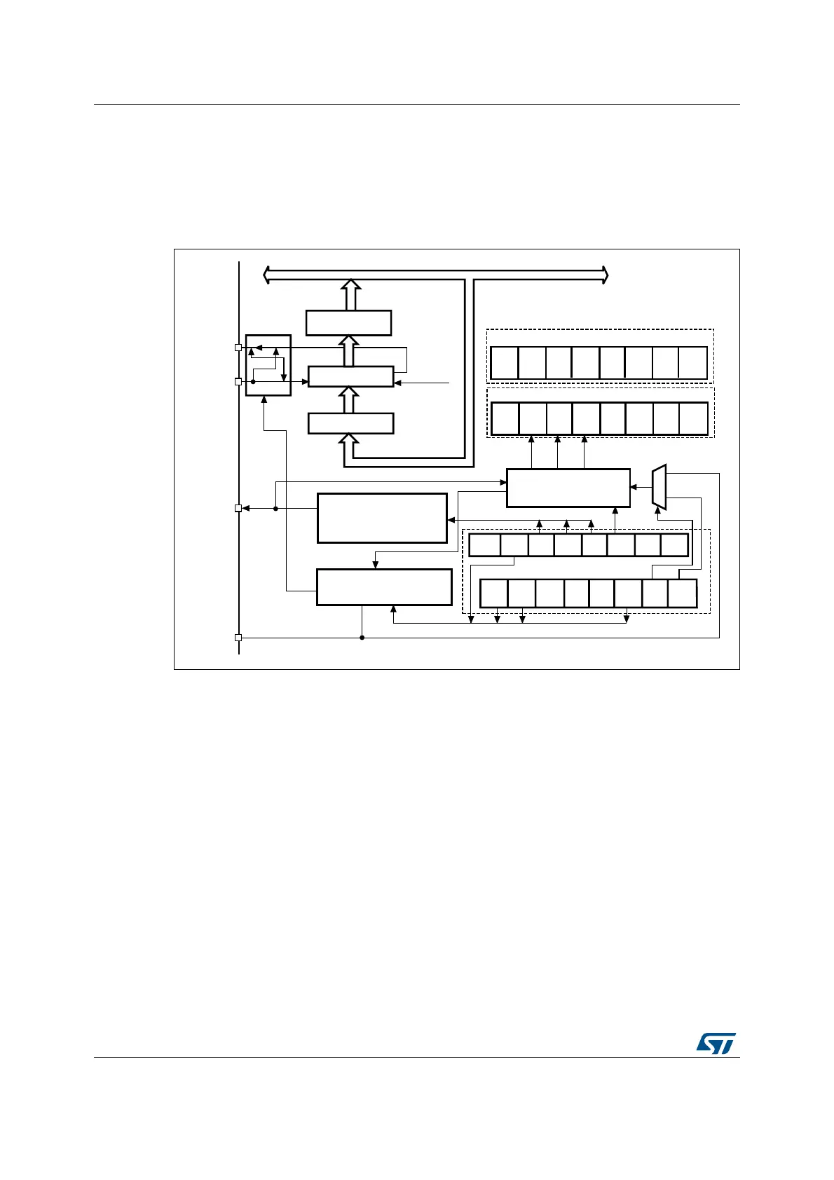
The block diagram of the SPI is shown in Figure 246.
Figure 246. SPI block diagram
Usually, the SPI is connected to external devices through four pins:
• MISO: Master In / Slave Out data. This pin can be used to transmit data in slave mode
and receive data in master mode.
• MOSI: Master Out / Slave In data. This pin can be used to transmit data in master
mode and receive data in slave mode.
• SCK: Serial Clock output for SPI masters and input for SPI slaves.
• NSS: Slave select. This is an optional pin to select a slave device. This pin acts as a
‘chip select’ to let the SPI master communicate with slaves individually and to avoid
contention on the data lines. Slave NSS inputs can be driven by standard IO ports on
the master device. The NSS pin may also be used as an output if enabled (SSOE bit)
and driven low if the SPI is in master configuration. In this manner, all NSS pins from
devices connected to the Master NSS pin see a low level and become slaves when
they are configured in NSS hardware mode. When configured in master mode with
NSS configured as an input (MSTR=1 and SSOE=0) and if NSS is pulled low, the SPI
enters the master mode fault state: the MSTR bit is automatically cleared and the
device is configured in slave mode (refer to Section 28.3.10).
A basic example of interconnections between a single master and a single slave is
illustrated in Figure 247.
MS51604V1
MOSI
MISO
Baud rate generator
SCK
Master control logic
Communication control
SPE BR2 BR1 BR0 MSTR CPOL CPHA
BR[2:0]
RXNE
IE
LSB
FIRST
BIDI
MODE
BIDI
OE
BSY OVR
MOD
F
RXNETXE
ERR
IE
TXE
IE
00
DFF
0 SSOE
CRCEN
0
RX
ONLY
CRC
Next
CRC
ERR
0
1
NSS
SPI_CR1
SPI_CR2
SPI_SR
TXDM
AEN
RXDM
AEN
Address and data bus
Read
Rx buffer
Shift register
LSB first
Tx buffer
Write
SSM SSI