RM0090 Rev 18 905/1749
RM0090 Serial peripheral interface (SPI)
925
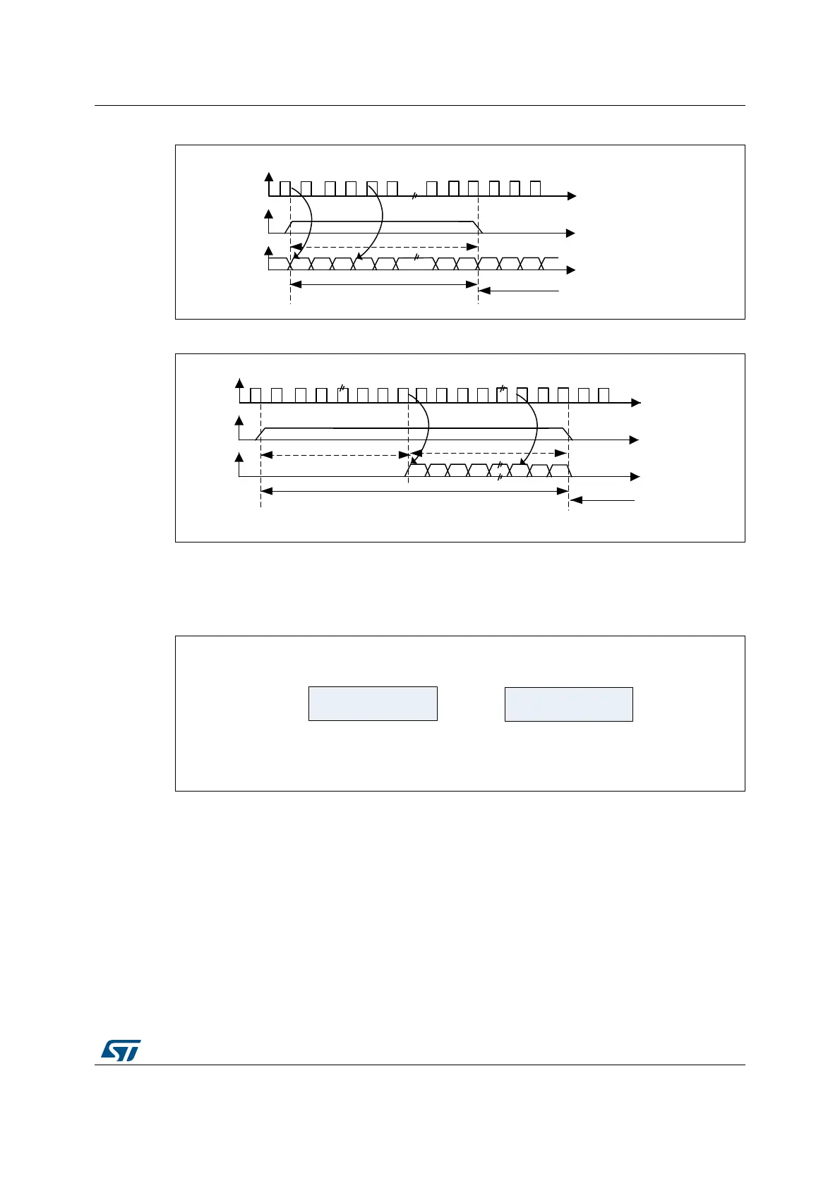
Figure 273. LSB justified 16-bit or 32-bit full-accuracy with CPOL = 0
Figure 274. LSB justified 24-bit frame length with CPOL = 0
• In transmission mode:
If data 0x3478AE have to be transmitted, two write operations to the SPI_DR register
are required from software or by DMA. The operations are shown below.
Figure 275. Operations required to transmit 0x3478AE
• In reception mode:
If data 0x3478AE are received, two successive read operations from SPI_DR are
required on each RXNE event.
MS30103V1
CK
WS
SD
Transmission
Reception
16- or 32-bit data
MSB
LSB
Channel left
Channel right
MSB
MS30104V1
CK
WS
SD
Transmission
Reception
8-bit data
0 forced
MSB
LSB
Channel left 32-bit
Channel right
24-bit remaining
0xXX34
0x78AE
First write to Data register
conditioned by TXE=1
Second write to Data register
conditioned by TXE=1
Only the 8 LSB of the
half-word are significant.
A field of 0x00 is forced
instead of the 8 MSBs.
MS19596V1