RM0090 Rev 18 1243/1749
RM0090 USB on-the-go full-speed (OTG_FS)
1380
34.3 OTG_FS functional description
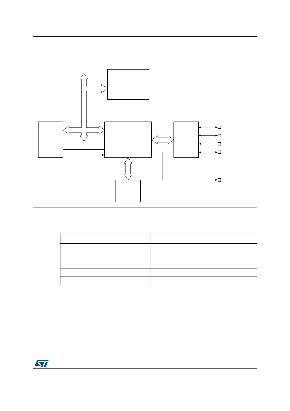
Figure 386. OTG full-speed block diagram
34.3.1 OTG pins
34.3.2 OTG full-speed core
The USB OTG FS receives the 48 MHz ±0.25% clock from the reset and clock controller
(RCC), via an external quartz. The USB clock is used for driving the 48 MHz domain at full-
speed (12 Mbit/s) and must be enabled prior to configuring the OTG FS core.
The CPU reads and writes from/to the OTG FS core registers through the AHB peripheral
bus. It is informed of USB events through the single USB OTG interrupt line described in
Section 34.15: OTG_FS interrupts.
MS19928V4
USB2.0
OTG FS
core
System clock domain
USB clock
domain
OTG
FS
PHY
OTG_FS_DP
OTG_FS_DM
OTG_FS_ID
OTG_FS_VBUS
Universal serial bus
Power
and
clock
controller
Cortex
®
core
UTMIFS
RAM bus
1.25 Kbyte
USB data
FIFOs
USB clock at 48 MHz
USB suspend
OTG_FS_SOF
Table 196. OTG_FS input/output pins
Signal name Signal type Description
OTG_FS_DP Digital input/output USB OTG D+ line
OTG_FS_DM Digital input/output USB OTG D- line
OTG_FS_ID Digital input USB OTG ID
OTG_FS_VBUS Analog input USB OTG VBUS
OTG_FS_SOF Digital output USB OTG Start Of Frame (visibility)