General-purpose I/Os (GPIO) RM0090
268/1749 RM0090 Rev 18
Each I/O port bit is freely programmable, however the I/O port registers have to be
accessed as 32-bit words, half-words or bytes. The purpose of the GPIOx_BSRR register is
to allow atomic read/modify accesses to any of the GPIO registers. In this way, there is no
risk of an IRQ occurring between the read and the modify access.
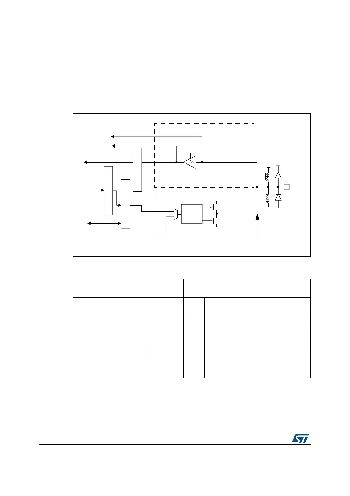
Figure 25 shows the basic structure of a 5 V tolerant I/O port bit. Table 39 gives the possible
port bit configurations.
Figure 25. Basic structure of a five-volt tolerant I/O port bit
1. V
DD_FT
is a potential specific to five-volt tolerant I/Os and different from V
DD
.
Table 35. Port bit configuration table
(1)
MODER(i)
[1:0]
OTYPER(i)
OSPEEDR(i)
[B:A]
PUPDR(i)
[1:0]
I/O configuration
01
0
SPEED
[B:A]
0 0 GP output PP
0 0 1 GP output PP + PU
0 1 0 GP output PP + PD
0 1 1 Reserved
1 0 0 GP output OD
1 0 1 GP output OD + PU
1 1 0 GP output OD + PD
1 1 1 Reserved (GP output OD)
Alternate function output
Alternate function input
Push-pull,
open-drain or
disabled
Output data register
Read/write
From on-chip
peripheral
To on-chip
peripheral
Output
control
Analog
on/off
Pull
Pull
on/off
I/O pin
V
DD
V
DD
V
SS
V
SS
TTL Schmitt
trigger
V
SS
V
DD_FT
(1)
Protection
diode
Protection
diode
on/off
Input driver
Output driver
down
up
P-MOS
N-MOS
Read
Bit set/reset registers
Write
Analog
Input data register
ai15939b