RM0090 Rev 18 117/1749
RM0090 Power controller (PWR)
149
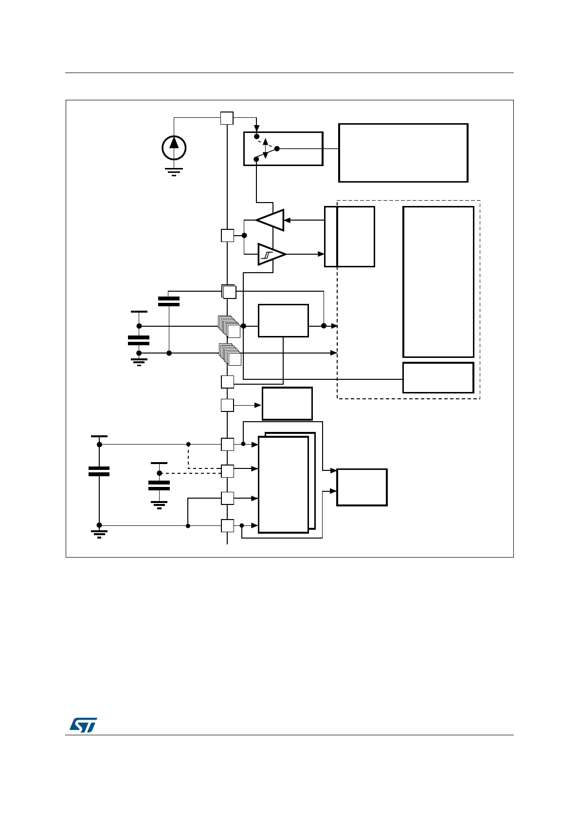
Figure 10. Power supply overview for STM32F42xxx and STM32F43xxx
1. V
DDA
and V
SSA
must be connected to V
DD
and V
SS
, respectively.
5.1.1 Independent A/D converter supply and reference voltage
To improve conversion accuracy, the ADC has an independent power supply which can be
separately filtered and shielded from noise on the PCB.
• The ADC voltage supply input is available on a separate V
DDA
pin.
• An isolated supply ground connection is provided on pin V
SSA
.
To ensure a better accuracy of low voltage inputs, the user can connect a separate external
reference voltage ADC input on V
REF
. The voltage on V
REF
ranges from 1.8 V to V
DDA
.
MS30482V2
V
DD
1/2/...14/20
Analo g:
RCs, PLL,
...
Power swi tch
V
BAT
GP I/Os
OUT
IN
Kernel logic
(CPU,
digital
& RAM)
Backup circuitry
(OSC32K,RTC,
Backup registers,
backup RAM)
Wakeup logic
19 × 100 nF
+ 1 × 4.7 μF
VBAT =
1.65 to 3.6V
Voltage
regulator
V
SS
1/2/...14/20
V
DDA
V
REF+
V
REF-
V
SSA
ADC
Level shifter
IO
Logic
V
DD
+ 1 μF
V
REF
100 nF
+ 1 μF
V
DD
Flash memory
V
CAP_1
V
CAP_2
2 × 2.2 μF
BYPASS_REG
PDR_ON
Reset
controller
100 nF