Secure digital input/output interface (SDIO) RM0090
1024/1749 RM0090 Rev 18
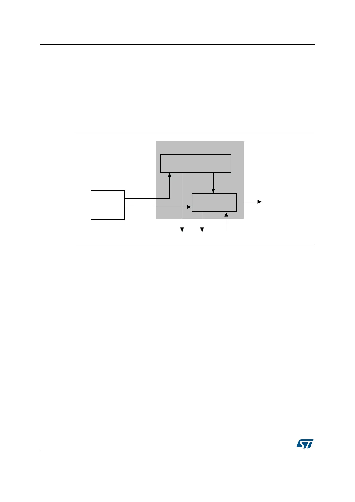
Control unit
The control unit contains the power management functions and the clock divider for the
memory card clock.
There are three power phases:
• power-off
• power-up
• power-on
Figure 328. Control unit
The control unit is illustrated in Figure 328. It consists of a power management subunit and
a clock management subunit.
The power management subunit disables the card bus output signals during the power-off
and power-up phases.
The clock management subunit generates and controls the SDIO_CK signal. The SDIO_CK
output can use either the clock divide or the clock bypass mode. The clock output is
inactive:
• after reset
• during the power-off or power-up phases
• if the power saving mode is enabled and the card bus is in the Idle state (eight clock
periods after both the command and data path subunits enter the Idle phase)
ai14804b
Control unit
Power management
Clock management
Adapter
registers
SDMMC_CK
To command and data path