Power controller (PWR) RM0090
124/1749 RM0090 Rev 18
Example of sequence 2:
1. Select HSI or HSE as system clock source.
2. Disable the peripheral clocks that are not generated by the System PLL (I2S clock,
LCD-TFT clock, SAI1 clock, USB_48MHz clock,....).
3. Reset the ODSW bit in the PWR_CR register to switch back the voltage regulator to
Normal mode. The system clock is stalled during voltage switching.
4. Wait for the ODWRDY flag of PWR_CSR to be reset.
5. Reset the ODEN bit in the PWR_CR register to disable the Over-drive mode.
Note: During step 3, the ODEN bit remains set and the Over-drive mode is still enabled but not
active (ODSW bit is reset). If the ODEN bit is reset instead, the Over-drive mode is disabled
and the voltage regulator is switched back to the initial voltage.
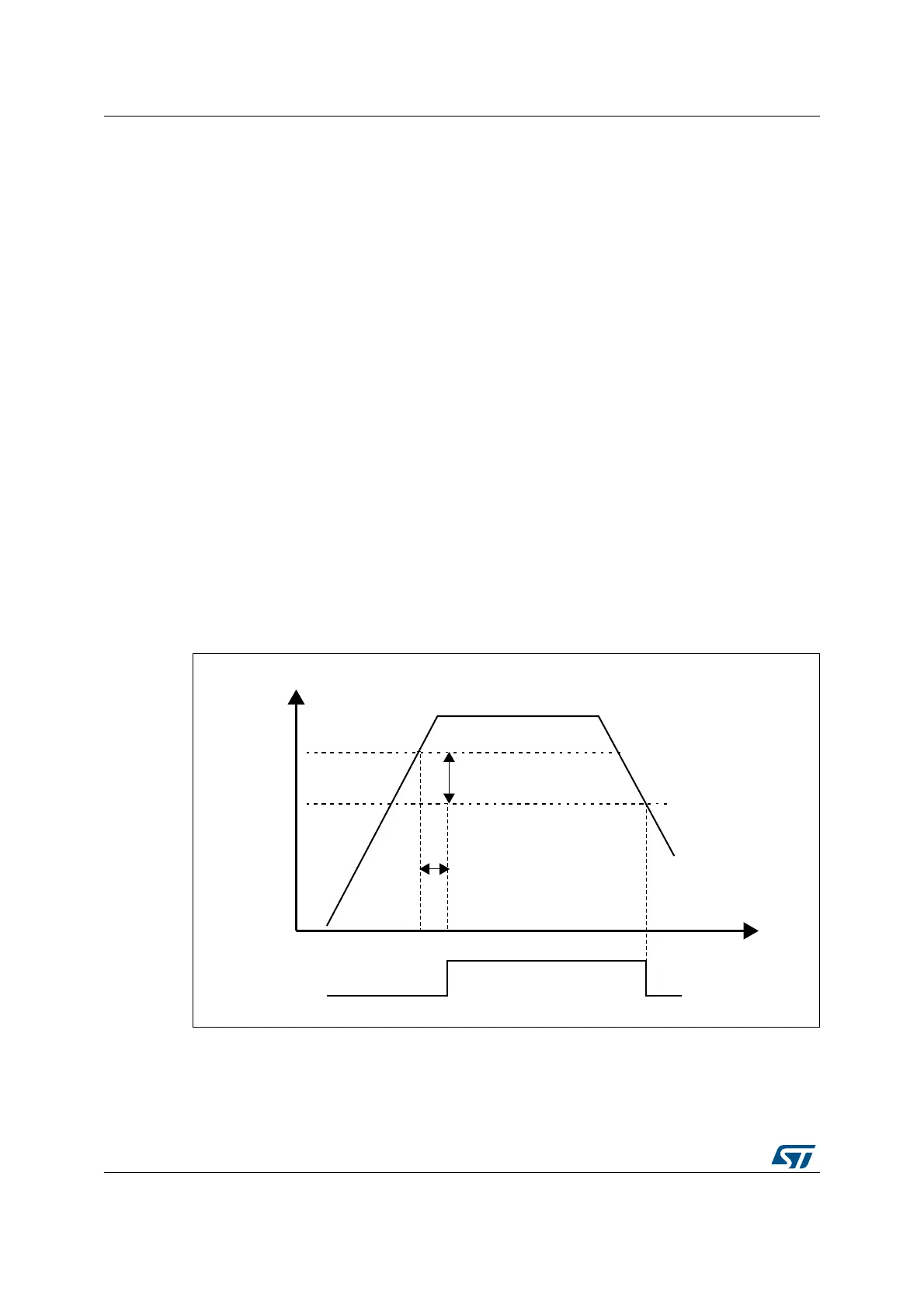
5.2 Power supply supervisor
5.2.1 Power-on reset (POR)/power-down reset (PDR)
The device has an integrated POR/PDR circuitry that allows proper operation starting
from 1.8 V.
The device remains in Reset mode when V
DD
/V
DDA
is below a specified threshold,
V
POR/PDR
, without the need for an external reset circuit. For more details concerning the
power on/power-down reset threshold, refer to the electrical characteristics of the
datasheet.
Figure 12. Power-on reset/power-down reset waveform
VDD/VDDA
40 mV
hysteresis
PDR
PDR
MS30431V1
Reset
Temporization
tRSTTEMPO