RM0090 Rev 18 481/1749
RM0090 LCD-TFT controller (LTDC)
514
16.3 LTDC functional description
16.3.1 LTDC block diagram
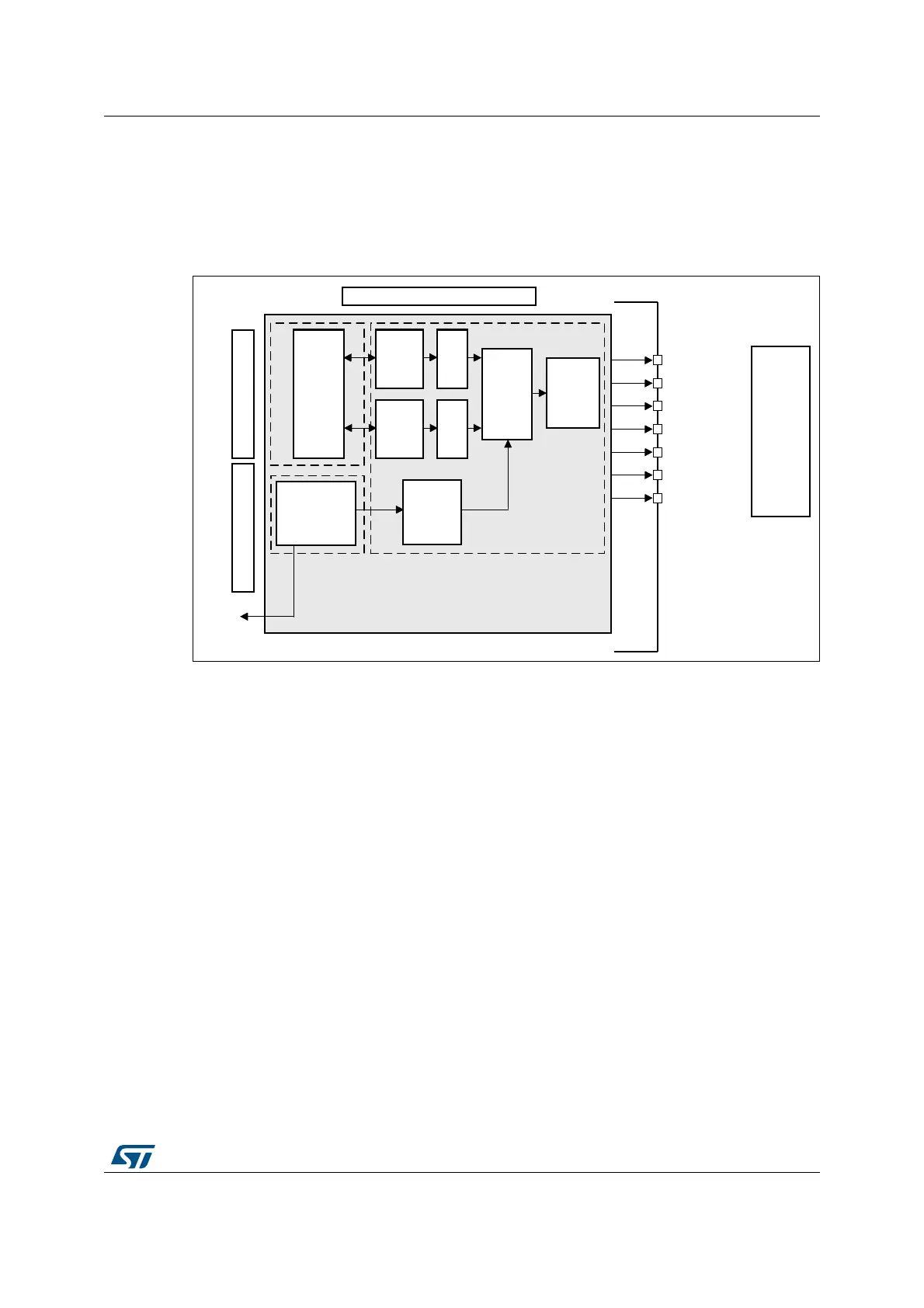
The block diagram of the LTDC is shown in Figure 81: LTDC block diagram.
Figure 81. LTDC block diagram
Layer FIFO: One FIFO 64x32 bit per layer.
PFC: Pixel Format Convertor performing the pixel format conversion from the selected input
pixel format of a layer to words.
AHB interface: For data transfer from memories to the FIFO.
Blending, Dithering unit and Timings Generator: Refer to Section 16.4.1 and Section 16.4.2.
16.3.2 LTDC reset and clocks
The LCD-TFT controller peripheral uses 3 clock domains:
• The AHB clock domain (HCLK) is used for data transfer from the memories to the
Layer FIFO and frame buffer configuration register
• The APB2 clock domain (PCLK2) is used for global configuration register and interrupt
registers
• The Pixel Clock domain (LCD_CLK) is used to generate LCD-TFT interface signals,
pixel data generation and layer configuration. The LCD_CLK output should be
configured following the panel requirements. The LCD_CLK is configured through the
PLLSAI (refer to RCC section).
Table 88 summarizes the clock domain for each register.
MSv19675V1
LCD-TFT
panel
LCD_HSYNC
LCD_VSYNC
LCD_DE
LCD_CLK
LCD_R[7:0]
LCD_G[7:0]
LCD_B[7:0]
Pixel clock domain
Dithering
unit
Blending
unit
PFC
PFC
Layer1
FIFO
Layer1
FIFO
AHB
interface
Timing
generator
Configuration
and status
registers
AHB clock domainAPB2 clock domain
Interrupts