Serial peripheral interface (SPI) RM0090
888/1749 RM0090 Rev 18
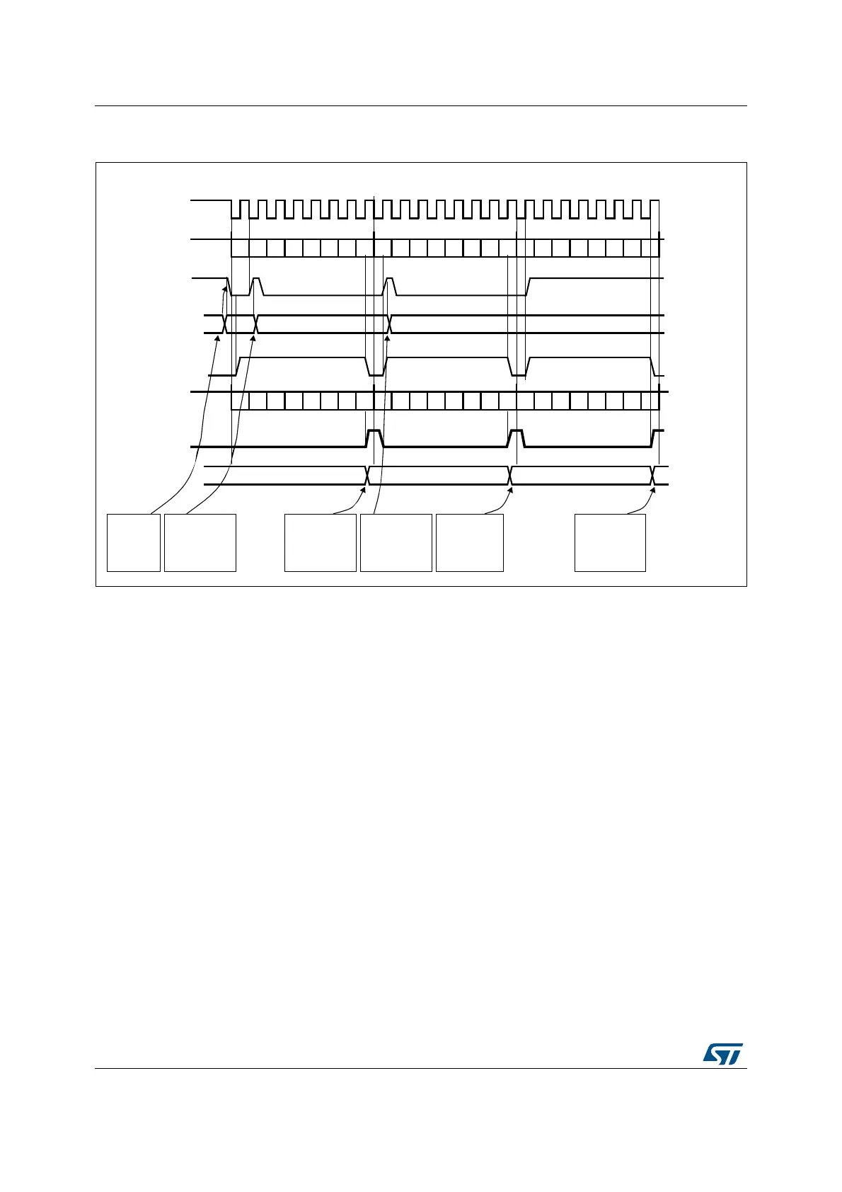
Figure 254. TXE/RXNE/BSY behavior in Slave / full-duplex mode (BIDIMODE=0,
RXONLY=0) in case of continuous transfers
Transmit-only procedure (BIDIMODE=0 RXONLY=0)
In this mode, the procedure can be reduced as described below and the BSY bit can be
used to wait until the completion of the transmission (see Figure 255 and Figure 256).
1. Enable the SPI by setting the SPE bit to 1.
2. Write the first data item to send into the SPI_DR register (this clears the TXE bit).
3. Wait until TXE=1 and write the next data item to be transmitted. Repeat this step for
each data item to be transmitted.
4. After writing the last data item into the SPI_DR register, wait until TXE=1, then wait until
BSY=0, this indicates that the transmission of the last data is complete.
This procedure can be also implemented using dedicated interrupt subroutines launched at
each rising edge of the TXE flag.
Note: During discontinuous communications, there is a 2 APB clock period delay between the
write operation to SPI_DR and the BSY bit setting. As a consequence, in transmit-only
mode, it is mandatory to wait first until TXE is set and then until BSY is cleared after writing
the last data.
After transmitting two data items in transmit-only mode, the OVR flag is set in the SPI_SR
register since the received data are never read.
0xF1
set by cleared by software
MISO/MOSI (in)
Tx buffer
DATA 1 = 0xA1
TXE flag
0xF2
BSY flag
0xF3
software
writes 0xF1
into SPI_DR
software waits
until TXE=1 and
writes 0xF2 into
SPI_DR
software waits
until RXNE=1
and reads 0xA1
from SPI_DR
set by hardware
cleared by software
set by hardware
cleared by software
set by hardware
SCK
DATA 2 = 0xA2
DATA 3 = 0xA3
reset by hardware
Example in Slave mode with CPOL=1, CPHA=1
RXNE flag
(write to SPI_DR)
Rx buffer
set by hardware
MISO/MOSI (out)
DATA 1 = 0xF1
DATA 2 = 0xF2
DATA 3 = 0xF3
(read from SPI_DR)
0xA1
0xA2 0xA3
software waits
until TXE=1 and
writes 0xF3 into
SPI_DR
software waits
until RXNE=1
and reads 0xA2
from SPI_ DR
software waits
until RXNE=1
and reads 0xA3
from SPI_DR
b0 b1 b2 b3 b4 b5 b6 b7 b0 b1 b2 b3 b4 b5 b6 b7 b0 b1 b2 b3 b4 b5 b6 b7
b0 b1 b2 b3 b4 b5 b6 b7 b0 b1 b2 b3 b4 b5 b6 b7 b0 b1 b2 b3 b4 b5 b6 b7
cleared by software
ai17344