RM0090 Rev 18 1665/1749
RM0090 Flexible memory controller (FMC)
1682
commands) are issued using the timing parameters configured for SDRAM Bank 1 (TMRD,
TRAS and TXSR timings) in the FMC_SDTR1 register.
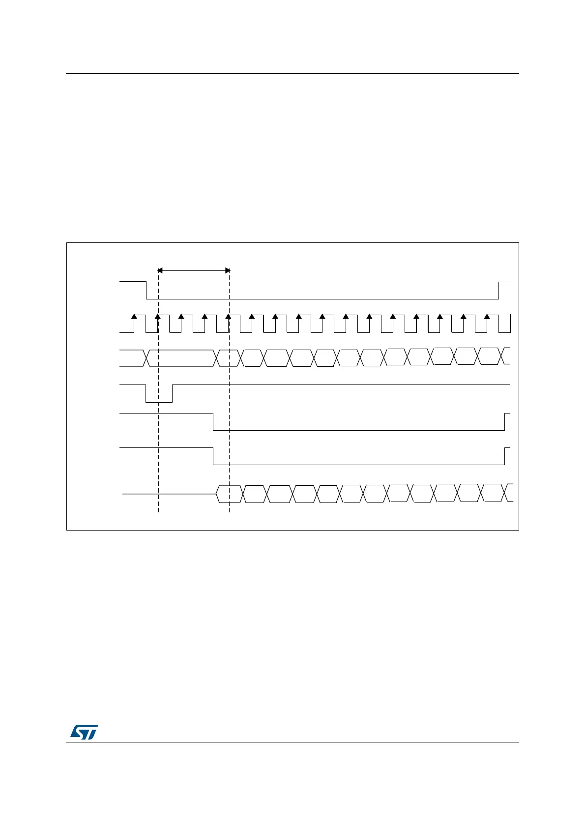
SDRAM controller write cycle
The SDRAM controller accepts single and burst write requests and translates them into
single memory accesses. In both cases, the SDRAM controller keeps track of the active row
for each bank to be able to perform consecutive write accesses to different banks (Multibank
ping-pong access).
Before performing any write access, the SDRAM bank write protection must be disabled by
clearing the WP bit in the FMC_SDCRx register.
Figure 478. Burst write SDRAM access waveforms
The SDRAM controller always checks the next access.
• If the next access is in the same row or in another active row, the write operation is
carried out,
• if the next access targets another row (not active), the SDRAM controller generates a
precharge command, activates the new row and initiates a write command.
MS30448V3
NRAS
A[12:0]
SDCLK
Row n Colc
SDNE
TRCD = 3
SDNWE
Cola Cold
Colb Cole
Colf Cog
Colh
Coli
Colj Colk Coll
NCAS
DATA[31:0]
Dnc
Dne
Dna Dnf
Dng Dnh
Dni
Dnj
Dnk Dnl
Dnb Dnd