RM0090 Rev 18 879/1749
RM0090 Serial peripheral interface (SPI)
925
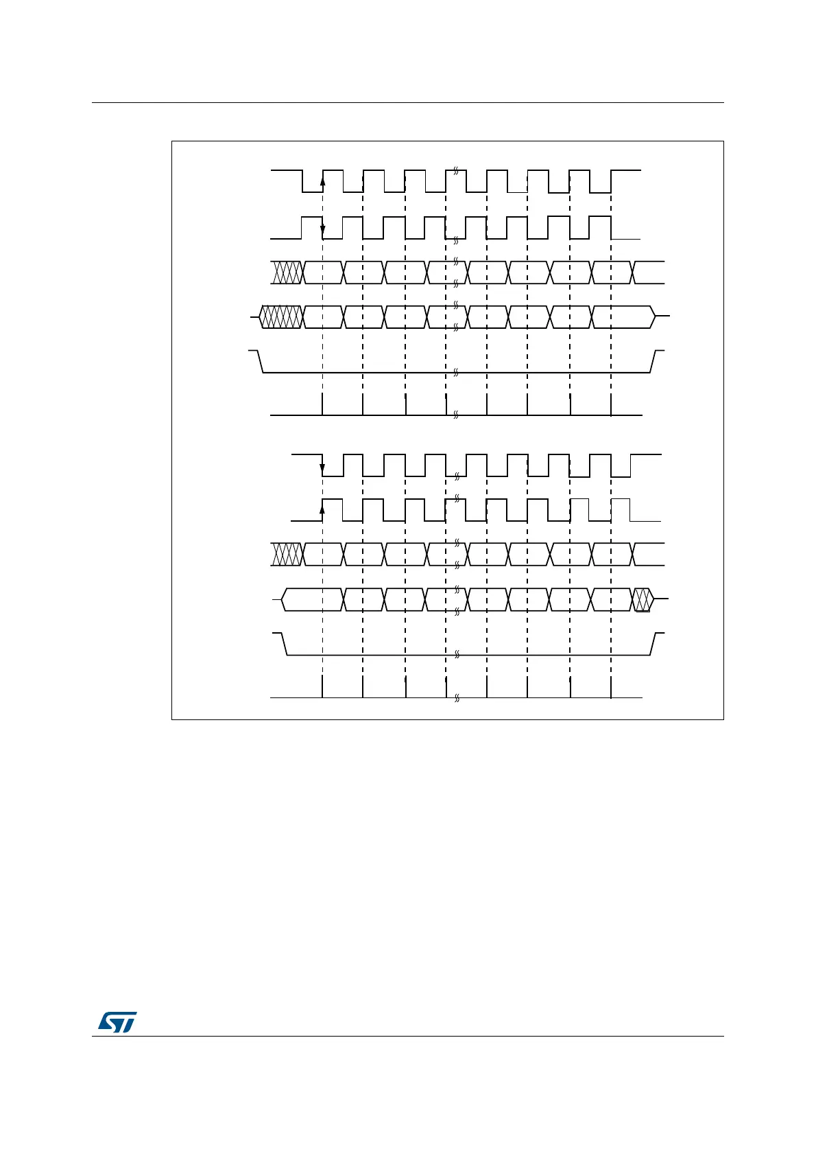
Figure 248. Data clock timing diagram
1. These timings are shown with the LSBFIRST bit reset in the SPI_CR1 register.
Data frame format
Data can be shifted out either MSB-first or LSB-first depending on the value of the
LSBFIRST bit in the SPI_CR1 Register.
Each data frame is 8 or 16 bits long depending on the size of the data programmed using
the DFF bit in the SPI_CR1 register. The selected data frame format is applicable for
transmission and/or reception.
CPOL = 1
CPOL = 0
MSBit
LSBit
MSBit
LSBit
MISO
MOSI
NSS
(to slave)
Capture strobe
CPHA =1
CPOL = 1
CPOL = 0
MSBit
LSBit
MSBit
LSBit
MISO
MOSI
NSS
(to slave)
Capture strobe
CPHA =0
ai17154d