RM0090 Rev 18 1545/1749
RM0090 Flexible static memory controller (FSMC)
1601
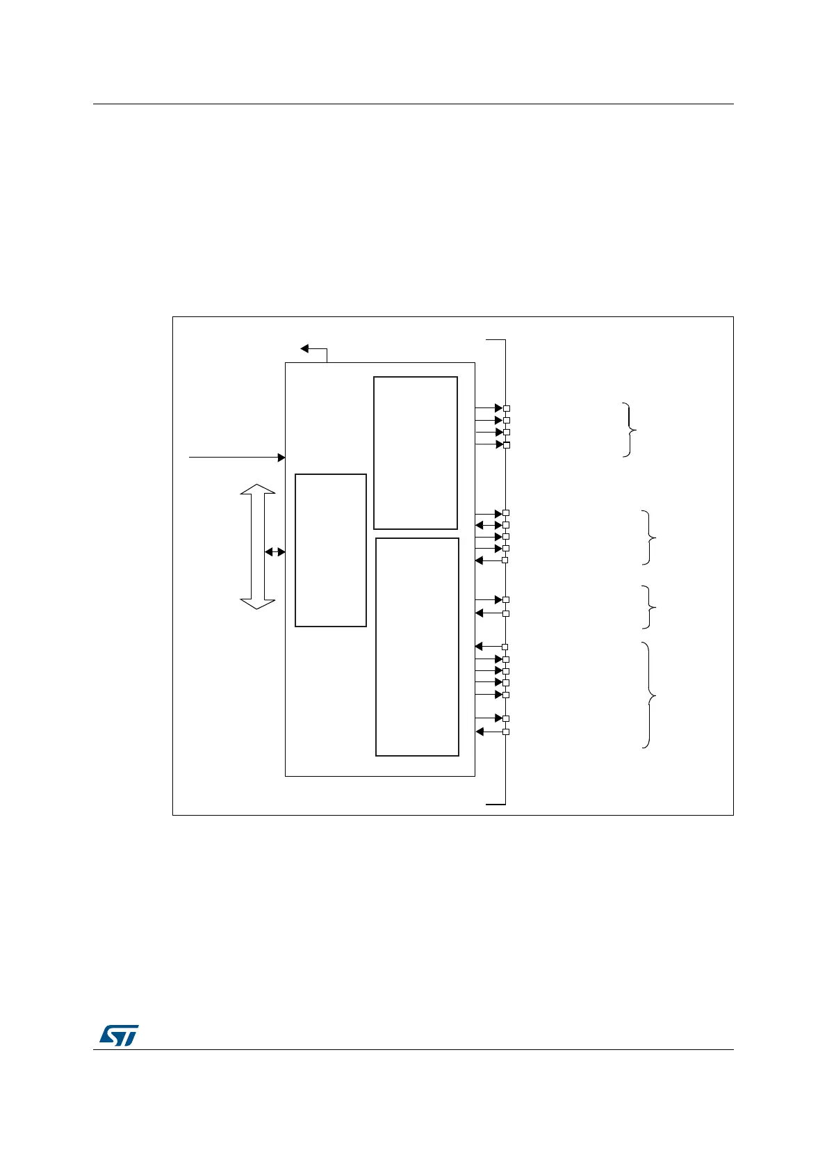
36.2 Block diagram
The FSMC consists of four main blocks:
• The AHB interface (including the FSMC configuration registers)
• The NOR Flash/PSRAM controller
• The NAND Flash/PC Card controller
• The external device interface
The block diagram is shown in Figure 434.
Figure 434. FSMC block diagram
36.3 AHB interface
The AHB slave interface enables internal CPUs and other bus master peripherals to access
the external static memories.
AHB transactions are translated into the external device protocol. In particular, if the
selected external memory is 16 or 8 bits wide, 32-bit wide transactions on the AHB are split
into consecutive 16- or 8-bit accesses. The FSMC Chip Select (FSMC_NEx) does not
AHB bus
FSMC interrupt to NVIC
NOR/PSRAM
memory
controller
HCLK
From clock
controller
NAND/PC Card
memory
controller
signals
NAND
Shared
signals
signals
NOR/PSRAM
FSMC_NE[4:1]
FSMC_NL (or NADV)
FSMC_NWAIT
FSMC_NOE
FSMC_NWE
FSMC_NIORD
FSMC_NREG
FSMC_CD
signals
PC Card
ai15591b
FSMC_NBL[1:0]
FSMC_NCE[3:2]
FSMC_INT[3:2]
FSMC_INTR
FSMC_NCE4_1
FSMC_NCE4_2
FSMC_NIOWR
FSMC_CLK
Configuration
registers
FSMC_A[25:0]
FSMC_D[15:0]